
Liquid metal rotating anode X-ray source for semiconductor metrology

a technology of liquid metal rotating anode and x-ray source, applied in the field of metalrology systems and methods, can solve the problems of difficult optical radiation penetration to the bottom layer, difficult characterization, and increased difficulty in characterization, so as to achieve effective self-healing, improve brightness and reliability, and increase the time interval between services

Active Publication Date: 2020-08-18
KLA CORP
View PDF74 Cites 3 Cited by
  • Summary
  • Abstract
  • Description
  • Claims
  • Application Information

AI Technical Summary

Benefits of technology

The patent is about a new type of X-ray source that uses a liquid metal material instead of a solid anode. This liquid metal material is not susceptible to cracking or degrading under repeated heating and cooling. This means that the X-ray source is more reliable and consistent over time. It also allows the X-ray source to stay in use for longer periods of time between maintenance, reducing downtime. Overall, this new X-ray source is much brighter and more reliable than traditional solid anode X-ray sources.

Problems solved by technology

As devices (e.g., logic and memory devices) move toward smaller nanometer-scale dimensions, characterization becomes more difficult.
Devices incorporating complex three-dimensional geometry and materials with diverse physical properties contribute to characterization difficulty.
For example, modern memory structures are often high-aspect ratio, three-dimensional structures that make it difficult for optical radiation to penetrate to the bottom layers.
As a result, the parameters characterizing the target often cannot be reliably decoupled with available measurements.
Optical radiation is often unable to penetrate layers constructed of these materials.
As a result, measurements with thin-film scatterometry tools such as ellipsometers or reflectometers are becoming increasingly challenging.
In response, more complex optical tools have been developed.
However, these approaches have not reliably overcome fundamental challenges associated with measurement of many advanced targets (e.g., complex 3D structures, structures smaller than 10 nm, structures employing opaque materials) and measurement applications (e.g., line edge roughness and line width roughness measurements).
Atomic force microscopes (AFM) and scanning-tunneling microscopes (STM) are able to achieve atomic resolution, but they can only probe the surface of the specimen.
In addition, AFM and STM microscopes require long scanning times. Scanning electron microscopes (SEM) achieve intermediate resolution levels, but are unable to penetrate structures to sufficient depth.
Thus, high-aspect ratio holes are not characterized well.
In addition, the required charging of the specimen has an adverse effect on imaging performance.
For example, transmission electron microscopes (TEM) achieve high resolution levels and are able to probe arbitrary depths, but TEM requires destructive sectioning of the specimen.
But, these techniques require sample destruction and lengthy process times. The complexity and time to complete these types of measurements introduces large inaccuracies due to drift of etching and metrology steps.
In addition, these techniques require numerous iterations which introduce registration errors.
Most research groups have employed high-brightness X-ray synchrotron sources which are not suitable for use in a semiconductor fabrication facility due to their immense size, cost, etc.
However, the resulting radiation is relatively low energy (92.6 electron volts), which severely limits the utility of these illumination sources in metrology applications.
Despite improved power loading capabilities, rotating anode sources suffer from significant limitations.
These microcracks introduce losses due to increased absorption.
In addition, in some examples, high rotation speeds limit X-ray spot size and spatial stability of the X-ray spot.
However, the liquid metal anode material does evaporate and form a metal vapor that may limit x-ray source lifetime.
In some examples, the metal vapor diffuses into the cathode region and contaminates the cathode, reducing cathode lifetime and system output.
In some examples, the metal vapor diffuses into the electron beam acceleration region causing high-voltage breakdowns.
Despite improved power loading capabilities, liquid anode sources suffer from significant limitations.
In practice, flowing thin liquid metal layers over other surfaces is limited to relatively low velocity flow.
As flow velocity increases, turbulence arises, which destabilizes the X-ray illumination source.
As a result, anode power loading of an X-ray source employing liquid anode material flowing over another surface is significantly limited.
In addition, anode power loading for X-ray illumination sources based on flowing liquid metal inside channels and tubes is limited by the structural integrity of any windows employed to contain the flow and allow electron beam penetration and X-ray extraction.
Therefore, any increase in jet speed to accommodate increased anode power loading is limited by the laminar-turbulent transition of the jet itself and the feasibility of an ultra-high-pressure jet return loop required to achieve any increased jet velocity.
Unfortunately, X-ray based metrology throughput is impaired by limited power loading on the anode.
An increase in power loading of a conventional solid metal anode source causes ablation and destruction of the anode.
For typical liquid metal sources, an increase in power loading tends to destabilize the X-ray illumination source.
Future metrology applications present challenges for metrology due to increasingly high resolution requirements, multi-parameter correlation, increasingly complex geometric structures, and increasing use of opaque materials.

Method used


Image

  • Liquid metal rotating anode X-ray source for semiconductor metrology
  • Liquid metal rotating anode X-ray source for semiconductor metrology
  • Liquid metal rotating anode X-ray source for semiconductor metrology

Examples


Embodiment Construction

[0047]Reference will now be made in detail to background examples and some embodiments of the invention, examples of which are illustrated in the accompanying drawings.

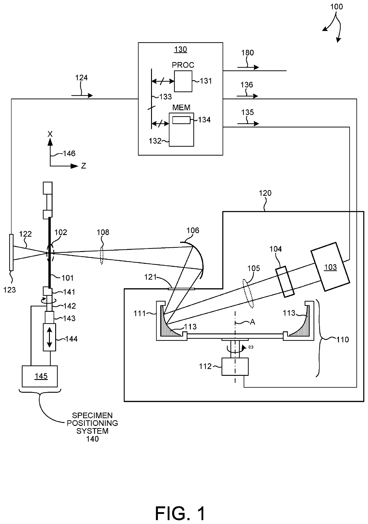
[0048]Systems employed to measure structural and material characteristics (e.g., material composition, dimensional characteristics of structures and films, etc.) associated with different semiconductor fabrication processes based on x-ray illumination are presented. More specifically, methods and systems for realizing a high brightness, liquid based x-ray source suitable for high throughput x-ray metrology are presented herein.

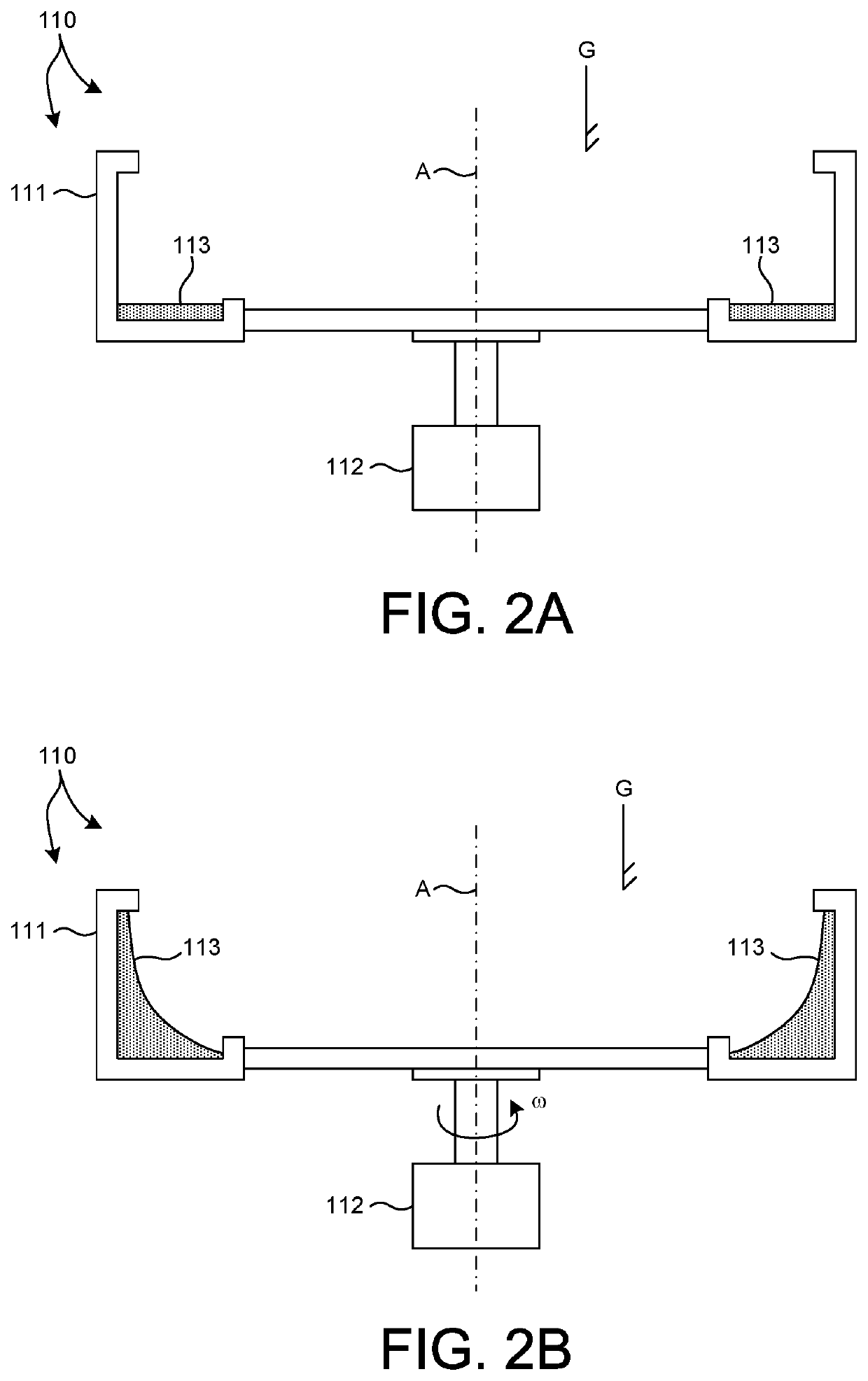
[0049]In one aspect, a high brightness x-ray source is produced by bombarding a rotating liquid metal anode material with a stream of electrons to generate x-ray radiation. The resulting x-ray emission is collected and provided to a semiconductor specimen to perform x-ray based metrology on the specimen.

[0050]The liquid metal material surface does not degrade (e.g., crack) under cyclic thermal s...


PUM

PropertyMeasurementUnit
roughnessaaaaaaaaaa
frequenciesaaaaaaaaaa
average poweraaaaaaaaaa

Abstract

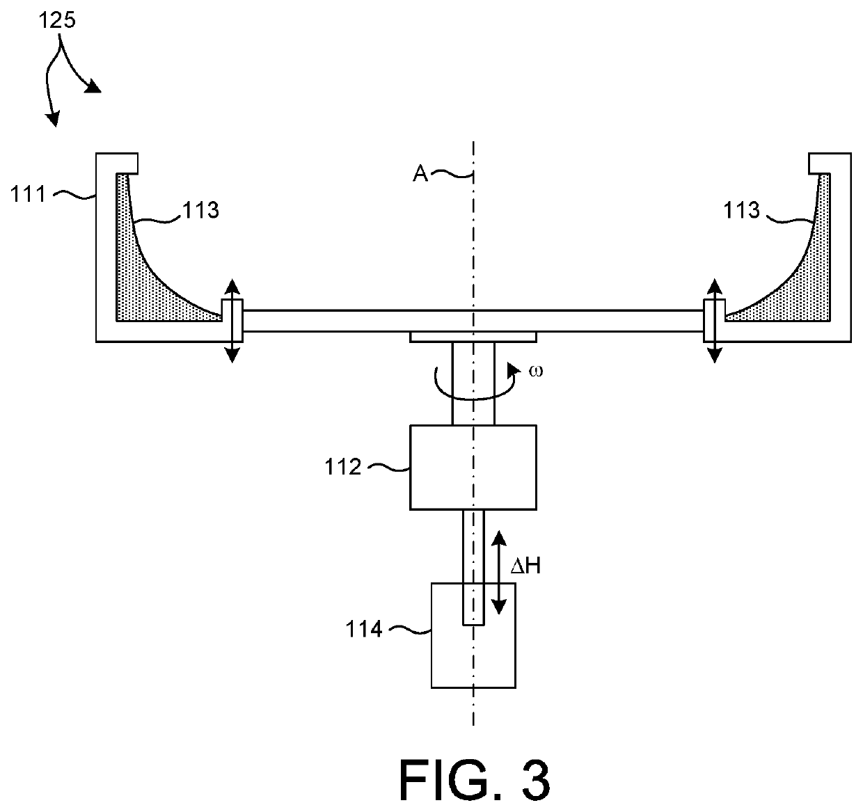
Methods and systems for realizing a high brightness, liquid based x-ray source suitable for high throughput x-ray metrology are presented herein. A high brightness x-ray source is produced by bombarding a rotating liquid metal anode material with a stream of electrons to generate x-ray radiation. A rotating anode support structure supports the liquid metal anode material in a fixed position with respect to the support structure while rotating at the constant angular velocity. In another aspect, a translational actuator is coupled to the rotating assembly to translate the liquid metal anode in a direction parallel to the axis of rotation. In another aspect, an output window is coupled to the rotating anode support structure. Emitted x-rays are transmitted through the output window toward the specimen under measurement. In another further aspect, a containment window maintains the shape of the liquid metal anode material independent of rotational angular velocity.

Description

CROSS REFERENCE TO RELATED APPLICATION[0001]The present application for patent claims priority under 35 U.S.C. § 119 from U.S. provisional patent application Ser. No. 62 / 573,958, entitled “X-Ray Source with Liquid Metal Rotating Anode (LiMeRa) for Semiconductor Metrology,” filed Oct. 18, 2017, the subject matter of which is incorporated herein by reference in its entirety.TECHNICAL FIELD[0002]The described embodiments relate to metrology systems and methods, and more particularly to methods and systems for improved illumination.BACKGROUND INFORMATION[0003]The various features and multiple structural levels of semiconductor devices such as logic and memory devices are typically fabricated by a sequence of processing steps applied to a specimen. For example, lithography among others is one semiconductor fabrication process that involves generating a pattern on a semiconductor wafer. Additional examples of semiconductor fabrication processes include, but are not limited to, chemical-me...

Claims


Application Information

Patent Timeline
Patent Type & Authority Patents(United States)
IPC IPC(8): H01J35/26H01J35/10G01N23/201G01N21/95H01J35/18H01L21/66
CPCH01J35/10G01N21/9501H01J35/101G01N23/201H01J35/105H01J35/18H01J2235/082H01J2235/1026H01L22/12G01B15/04
Inventor ZALUBOVSKY, SERGEY
Owner KLA CORP
Learn More