Method for fabricating mos transistors

a transistor and mos technology, applied in the direction of transistors, semiconductor devices, electrical equipment, etc., can solve the problems of boron implantation, boron introduction into silicon film, and difficult control of short channel effect,

Inactive Publication Date: 2001-08-09
SONY CORP
View PDF0 Cites 36 Cited by
  • Summary
  • Abstract
  • Description
  • Claims
  • Application Information

AI Technical Summary

Benefits of technology

0035] Specifically, to attain its object as above, the invention provides a method for fabricating MOS transistors, which comprises a step of forming a gate electrode of a p-type silicon film on a gate insulating film as formed on the surface of a semiconductor substrate, and a step of forming a silicon nitrid

Problems solved by technology

However, in such embedded channel-type MOS transistors, the tip of the depletion layer extending from the source/drain region is too near to another one adjacent thereto in the deep part of the substrate, as being influenced by the gate electric field, thereby often causing punch-through.
This means the difficulty in controlling the short channel effect in coming deep sub-micron generation devices in the art.
However, the boron implantation is problematic in that the boron introduced into the silicon film often diffuses away when the substrate is exposed to high temperatures in subsequent steps.
At present, however, it is extremely difficult to form a silicon nitride film not containing hydrogen, and it is therefore also difficult to retard the boron diffusion that shall be accelerated by hydrogen.
However, the former is problematic in that the crystal defects as caused by ion implantation or dry etching could not be restored sufficien

Method used


Image

  • Method for fabricating mos transistors
  • Method for fabricating mos transistors
  • Method for fabricating mos transistors

Examples


example 1

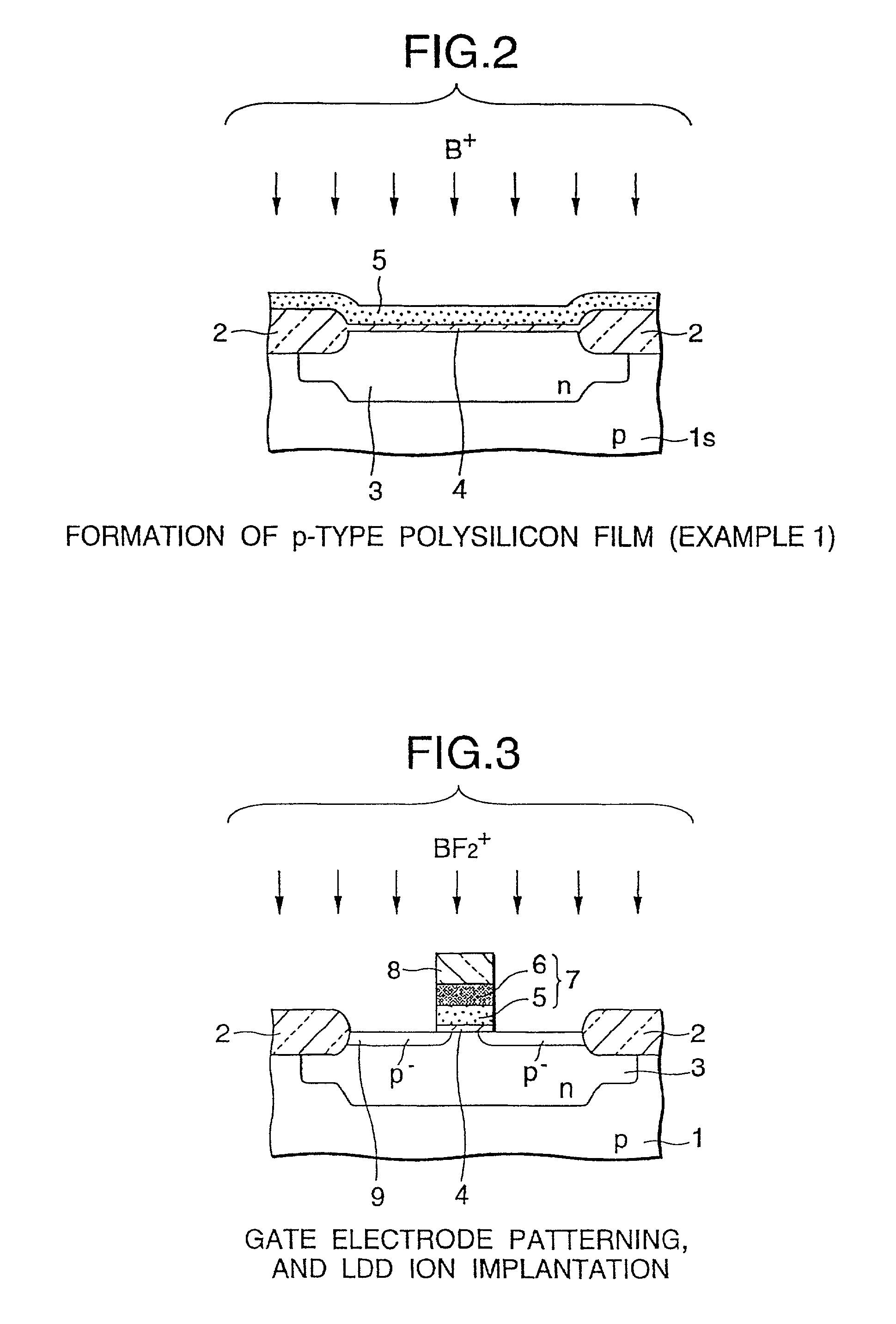
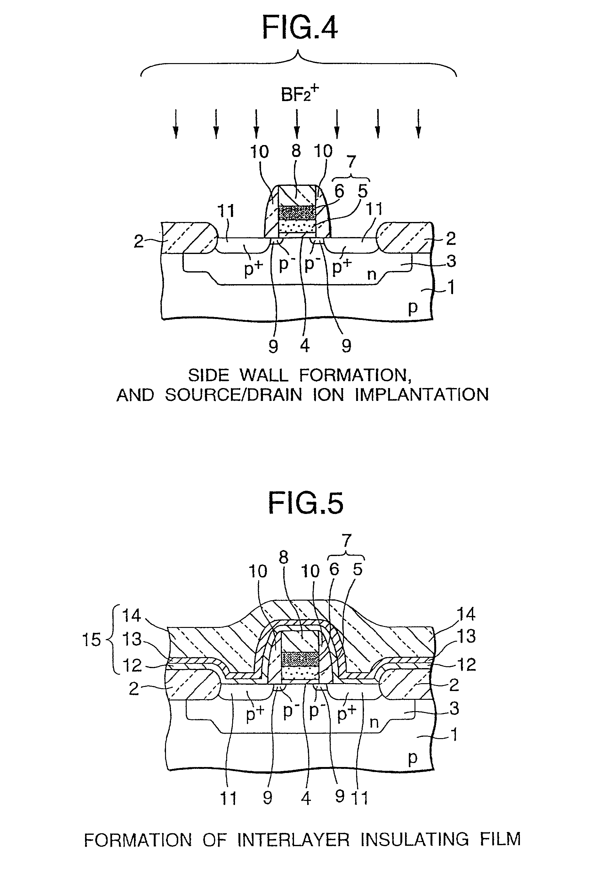
[0069] This is one embodiment of the invention as applied to a process of fabricating a PMOS structure that contains a silicon nitride film as a part of the interlayer insulating film, for which referred to are FIG. 2 to FIG. 6.

[0070] First, elements on a p-type Si substrate 1 were spaced from each other according to a known LOCOS process. Concretely, for example, a field oxide film 2 was formed on the substrate 1 through wet oxidation at 950.degree. C.

[0071] Next, an n-type well 3 was formed through p.sup.+ ion implantation via a resist mask (not shown) in the PMOS forming region. For the condition for the ion implantation, for example, the ion accelerating energy was 330 keV, and the ion dose was 8.times.10.sup.12 / cm.sup.2 .

[0072] Next, after ion implantation in the surface layer part of the active region for threshold voltage (V.sub.th) control followed by ion implantation in the depth of the substrate for forming therein an embedded layer for punch-through retardation, the subst...

example 2

[0098] This is another embodiment of the invention as applied to a self-aligned contact process of fabricating a DRAM structure, for which referred to are FIG. 7 to FIG. 10. In those drawings, some numeral references are the same as those in FIG. 2 to FIG. 6 referred to hereinabove.

[0099] Two gate electrodes 7 as in Example 1 were formed adjacent to each other in an element forming region. Also as in Example 1, an LDD region 9, a side wall 10 and a source / drain region 11 were formed. In DRAM, the gate electrodes 7 function as word lines.

[0100] Next, a silicon oxide film 12, a silicon nitride film 13 and a silicon oxide film 14 were layered in that order to form an interlayer insulating film 15.

[0101] The silicon oxide film 12 was formed, for example, through reduced pressure CVD at 720.degree. C., for which was used a mixed gas of TEOS / O.sub.2, and it had a thickness of about 20 nm.

[0102] The silicon nitride film 13 was formed, for example, through reduced pressure CVD at 760.degree...

example 3

[0112] This is still another embodiment of the invention as applied to a SALICIDE process of fabricating a dual gate CMOS structure, for which referred to are FIG. 11 to FIG. 16.

[0113] FIG. 11 shows the condition of a substrate having been subjected to element spacing, well formation and gate oxidation, in which a polysilicon film formed on the substrate was patterned to give a gate electrode 21 in the PMOS forming region and a gate electrode 22 in the NMOS forming region, and thereafter the PMOS forming region was subjected to LDD ion implantation with BF.sub.2.sup.+ while the NMOS forming region was masked with a resist pattern 23.

[0114] The gate electrodes 21 and 22 were formed, for example, as follows: A polysilicon film was deposited through reduced pressure CVD with SiH.sub.4 gas at a temperature falling between 580 and 620.degree. C. to have a thickness of from 150 to 300 nm, and this was then patterned through anisotropic dry etching with a mixed gas of Cl.sub.2 / O.sub.2.

[011...


PUM


Abstract

In PMOS having a gate electrode 7 of a p-type polysilicon film 5 along with a silicon nitride film 13, boron diffusion from the p-type polysilicon film 5 and boron punching through the gate oxide film 4 are prevented, thereby stabilizing the properties of the PMOS. Hydrogen existing in the silicon nitride film 13 accelerates boron diffusion from the film 5. To prevent it, all subsequent steps after the step of forming the silicon nitride film 13 are effected within a temperature range within which the boron diffusion is not accelerated by hydrogen. Forming the silicon oxide film 14 through reduced pressure CVD is effected in a furnace at a temperature lower than 850.degree. C. Annealing for dopant activation in the compensation region 17 to be formed on the substrate in the bottom of the contact hole 16 is effected in a manner of RTA (rapid thermal annealing) at a temperature lower than 1000.degree. C.

Description

BACKGROUND OF THE INVENTION[0001] 1. Field of the Invention[0002] The present invention relates to a method for fabricating MOS transistors, in particular to a method for fabricating MOS transistors having both a p-type gate electrode of a p-type MOS transistor (PMOS) and a silicon nitride film on a substrate, in which boron (B) in the p-type gate electrode is effectively prevented from diffusing away and from punching through the adjacent gate oxide film.[0003] 2. Description of the Related Art[0004] Complementary MOS transistor (CMOS) circuits having both an N-type MOS transistor (NMOS) and a p-type MOS transistor (PMOS) on one and the same substrate have the advantages of reduced power consumption and quick operation as fine patterning to increase the degree of integration in fabricating them is easy, and they have many applications, for example, for memory units and logical units and for other various LSI devices.[0005] Various films of n.sup.+-type polysilicon films as well as ...

Claims


Application Information

Patent Timeline
IPC IPC(8): H01L29/78H01L21/285H01L21/336H01L21/60H01L21/768H01L21/8238H01L27/092
CPCH01L21/28518H01L21/76801H01L21/76814H01L21/76832H01L21/76834H01L21/76897H01L29/6659H01L29/78
Inventor TSUKAMOTO, MASANORI
Owner SONY CORP
Why Eureka
Try Eureka