Method of forming dual damascene structure

a damascene and structure technology, applied in the direction of semiconductor devices, semiconductor/solid-state device details, electrical equipment, etc., can solve the problems of low dielectric constant film damage, high production cost, and same problem

Inactive Publication Date: 2002-10-03
JSR CORPORATIOON
View PDF3 Cites 33 Cited by
  • Summary
  • Abstract
  • Description
  • Claims
  • Application Information

AI Technical Summary

Problems solved by technology

Because of these steps, the via-first method has a problem that the low dielectric constant film is unavoidably damaged by the plasma or potent wet stripping liquid used for removing the residue of the resist or antireflection film filling the via.
The trench-first method has the same problem.
However, it has a problem that the production cost is high because the substrate need to shuttle many times between a film deposition step and a lithographic step.
However, this technique has a problem that since all these films are silicon-containing films, it is difficult to secure a sufficient etching selective ratio between the layers to form a dual damascene structure having a satisfactory shape.
This technique further has a drawback that when it is used in combination with film formation from a coating material, a silicon wafer shuttles between the coating apparatus for film formation from a coating fluid and the CVD apparatus, making the process flow complicated.
On the other hand, in case where the content thereof exceeds 60% by weight, the coating fluid gives a film which has too high water-absorbing properties and reduced electrical properties.
Furthermore, in case where the amount by weight of the product of hydrolysis and condensation derived from the compound (1) is not smaller than that of the product of hydrolysis and condensation derived from the compound (2), the coating fluid gives a film having poor strength.
Because of this, use of an organic dielectric film having a glass transition point lower than 400.degree. C. is undesirable in that it may deform during multilayer wiring to pose problems such as wiring connection failures and delamination.

Method used


Image

  • Method of forming dual damascene structure
  • Method of forming dual damascene structure

Examples


synthesis example 2

[0118] Preparation of Coating Fluid for Organic Dielectric film

[0119] Into a flask were introduced 37.8 g of 9,9-bis(4-hydroxy-3-methylph-enyl)fluorene and 37.8 g of potassium carbonate together with 350 g of dimethylacetamide. The contents were heated at 150.degree. C. for 2 hours in a nitrogen atmosphere while removing the resulting water vapor from the system. To this solution was added 21.8 g of bis(4-fluorophenyl) ketone. The resulting mixture was reacted at 165.degree. C. for 10 hours, subsequently cooled, and then filtered to remove the insoluble matter contained in the solution. Reprecipitation was conducted from methanol. This precipitate was sufficiently washed with ion-exchanged water and then dissolved in cyclohexanone. After the insoluble matter was removed, the solution was poured into methanol to conduct reprecipitation. This precipitate was dried in a 60.degree. C. vacuum oven for 24 hours to obtain a polymer.

[0120] In 18 g of cyclohexanone was dissolved 2 g of the p...

synthesis example 3

[0121] Preparation of Coating Fluid for Metal Oxide Film Formation

[0122] (1) In 298 g of propylene glycol monopropyl ether was dissolved 106.4 g of tetramethoxysilane. This solution was stirred with a Three-One Motor to keep the solution temperature at 60.degree. C. Subsequently, 50 g of ion-exchanged water containing 2.1 g of maleic acid dissolved therein was added to the solution over 1 hour. Thereafter, the reaction mixture was reacted at 60.degree. C. for 4 hours and then cooled to room temperature. A solution containing methanol was removed in an amount of 90 g from the reaction mixture at 50.degree. C. by evaporation, and 643 g of propylene glycol monopropyl ether was added to the residue to obtain a solution (A).

[0123] (2) To the solution (A) was added 5 g of bis(4-t-butylphenyl)iodoni-um camphorsulfonate as ingredient (B). The resulting mixture was filtered through a Teflon filter having a pore diameter of 0.2 .mu.m to obtain a coating fluid for metal oxide film formation.

example 1

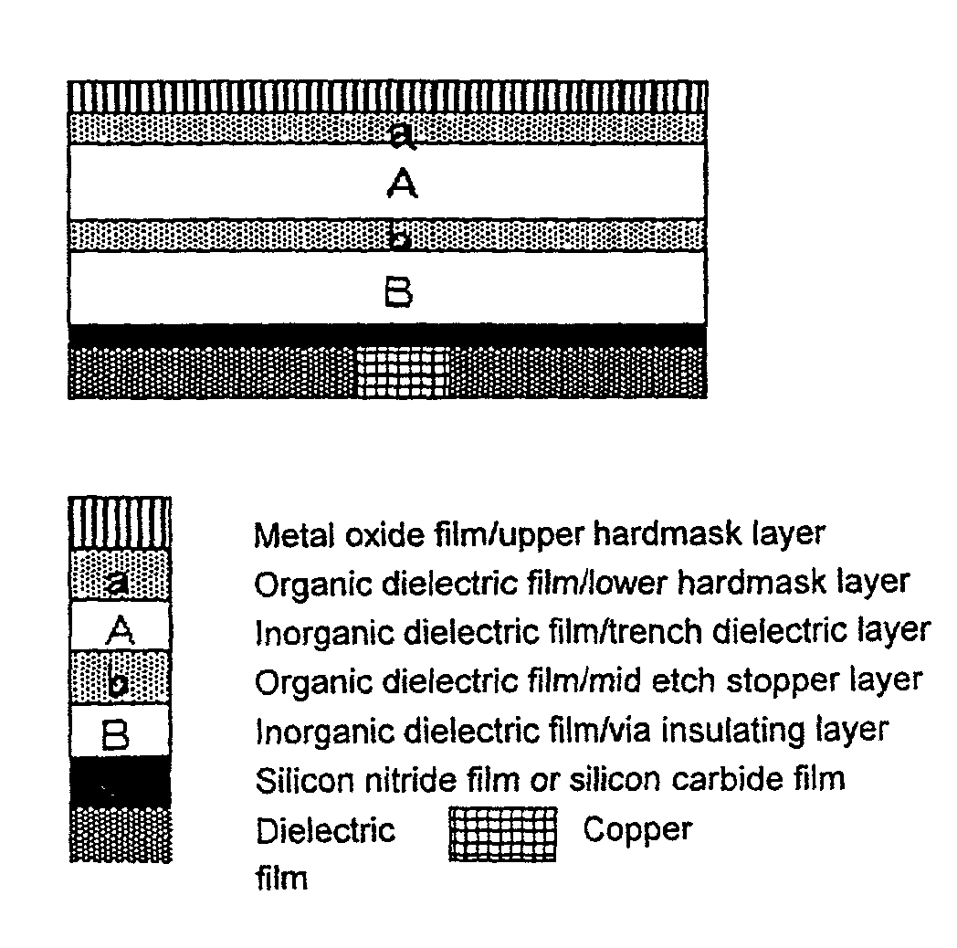
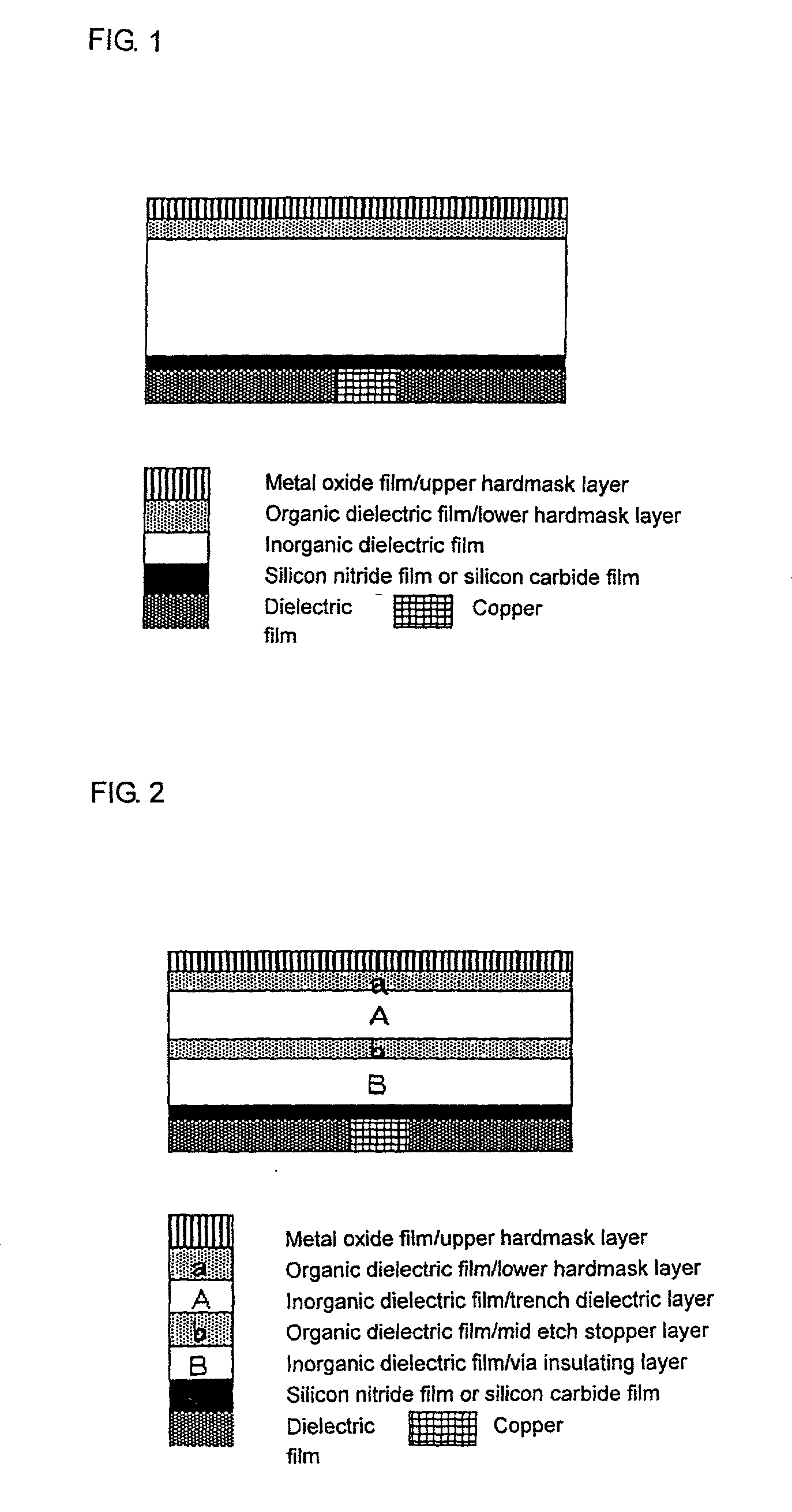
[0124] (1) A silicon nitride film having a thickness of 400 nm was formed on a silicon substrate by ordinary plasma CVD. The coating fluid for inorganic dielectric film formation prepared in Synthesis Example 1 was applied to the coated substrate by spin coating, and this substrate was heated first in the air at 80.degree. C. for 5 minutes and subsequently in nitrogen at 200.degree. C. for 5 minutes and then heated under vacuum at 425.degree. C. for 1 hour to thereby form a via insulating layer (A) composed of an inorganic dielectric film having a thickness of 300 nm.

[0125] The via insulating layer formed was subjected to a UV / ozone treatment to activate the surface thereof. Thereafter, the coating fluid for organic dielectric film formation prepared in Synthesis Example 2 was applied thereto by spin coating. This substrate was dried first at 80.degree. C. for 1 minute and subsequently at 200.degree. C. for 2 minutes and then further heated in a 450.degree. C. nitrogen atmosphere fo...


PUM

PropertyMeasurementUnit
dielectric constantaaaaaaaaaa
temperatureaaaaaaaaaa
glass transition pointaaaaaaaaaa

Abstract

A method of dual damascene structure formation suitable for wiring on semiconductors. The method of forming a dual damascene structure includes the steps of forming an organic dielectric film and a metal oxide film on an inorganic dielectric film, forming a pattern on the resulting multilayer structure, and then etching the structure.

Description

[0001] The present invention relates to a method of wiring for semiconductor devices. More particularly, the invention relates to a dual damascene structure suitable for wiring on semiconductors and to a method of forming the same.DESCRIPTION OF THE RELATED ART[0002] With the trend toward size reduction in semiconductor devices, the shifting of the wiring material from aluminum, which has been used hitherto, to copper is progressing. In the case of using copper as an interconnect material, damascene methods are frequently used. Of these methods, the dual damascene method, by which a via-post and trench line can be simultaneously formed, is regarded as a preferred technique because it is effective in reducing the semiconductor device production cost.[0003] The technique of forming a copper wiring by the dual damascene method is presently spreading and coming to be generally used for forming interconnect structures containing SiO.sub.2 as dielectrics.[0004] The desire for further size...

Claims


Application Information

Patent Timeline
Patent Type & Authority Applications(United States)
IPC IPC(8): H01L21/312H01L21/316H01L21/28H01L21/768H01L23/522
CPCH01L21/0212H01L21/02126H01L21/022H01L21/02216H01L21/02282H01L21/02337H01L21/76835H01L21/3121H01L21/3127H01L21/316H01L21/76811H01L21/76829H01L21/02348H01L21/28
Inventor SHIOTA, ATSUSHI
Owner JSR CORPORATIOON
Why Eureka
Try Eureka