Method of preparing optically imaged high performance photomasks
a high-performance, optical image technology, applied in the direction of photomechanical treatment originals, photomechanical instruments, photomechanical equipment, etc., can solve the problems of difficult to do the metrology which is used to determine whether the finished reticle is finished or not, and the critical dimension is uniform across the reticle substrate surface, and achieves long stability period and uniformity. , the effect of uniformity
- Summary
- Abstract
- Description
- Claims
- Application Information
AI Technical Summary
Benefits of technology
Problems solved by technology
Method used
Image
Examples
example one
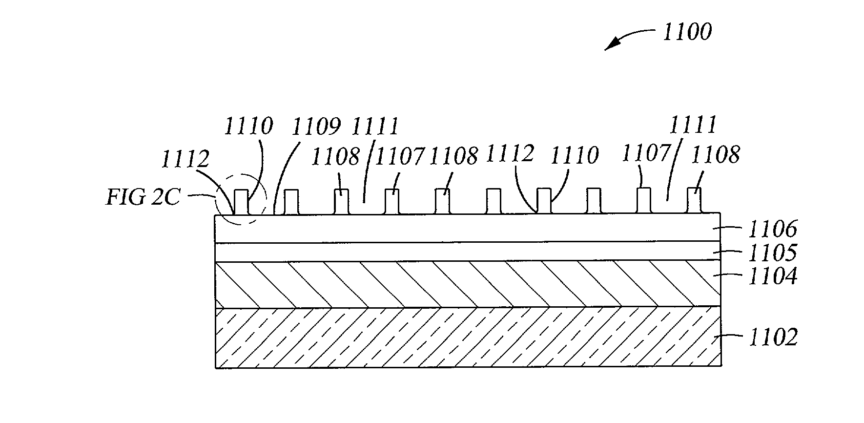
[0064] FIG. 11A shows a starting structure 1100 used in the fabrication of a photomask, hereafter referred to as a reticle. In this Example, starting structure 1100 was a stack of layers (not shown to scale) which included, from top to bottom, a 5,000 .ANG. thick layer 1108 of a chemically amplified DUV photoresist, DX1100 (available from AZ Clariant Corp. of Somerville, N.J.); a 470 .ANG. thick layer 1106 of an organic ARC identified as KRF 17G (available from AZ / Clariant); a 250 .ANG. thick layer 1105 of chromium oxynitride inorganic ARC; a 750 .ANG. thick layer 1104 of chrome mask material; and a silicon oxide-containing substrate 1102.
[0065] In particular, the chemically amplified DUV photoresist, DX1100, comprises propylene glycol monomethyl ether acetate (PGMEA); PMA; 1-methoxy-2-propyl acetate; modified phenolic polymer; and an onium salt metal halide complex as a chemical amplifier. This DUV photoresist is applied over the surface of underlying organic ARC layer 1106 in the ...
example two
[0093] FIG. 12A shows a starting structure 1200 used in the fabrication of a photomask (reticle). In this Example, starting structure 1200 is a stack of layers which included, from top to bottom, a 5,000 .ANG. thick layer 1208 of the chemically amplified DUV photoresist, DX1100; a 540 .ANG. thick layer 1206 of the organic ARC KRF 17G; a 750 .ANG. thick layer 1204 of a mask material which is essentially chrome; and a silicon oxide-containing substrate 1202.
[0094] FIG. 12B shows a schematic cross-sectional view of the patterned photoresist layer 1208 (prior to transfer of the pattern through underlying organic ARC layer 1206, and chrome-containing layer 1204), where the pattern is lines 1207 and spaces 1211, where the line width is about 0.30 .mu.m and the spacing between lines is about 0.3 .mu.m. The patterning is done using the direct write continuous wave laser, in particular, the 257 nm mask writing laser tool available from ETEC Systems which was described above. The patterning m...
example three
[0102] During the development of correlations between the PAB and PEB and critical dimension sensitivity and uniformity, applicants discovered that an increased shelf life can be obtained for photoresist coated photomask / reticle substrates prior to imaging (prior to exposure to radiation for patterning). An increased shelf life for these photoresist coated substrates is particularly important, since the manufacturer for the coated substrates is typically not the same as the manufacturer who exposes the coated substrates to radiation to create an image in the photoresist.
[0103] FIG. 3 shows a graph 300 of the critical dimension in nm obtained in chrome when a photoresist-coated (193 nm chemically amplified photoresist from Tokyo Ohka America, having offices in Hillsboro, Oreg.) photomask substrate was stored in ambient atmosphere in a clean room at room temperature prior to exposure to radiation for imaging. The PAB used after application of the photoresist was 90.degree. C. for 60 s...
PUM
 Abstract
Description
Claims
Application Information


