Externally excited torroidal plasma source with magnetic control of ion distribution

a plasma source and magnetic control technology, applied in the field of externally excited torroidal plasma sources with magnetic control of ion distribution, can solve the problems of slow and therefore relatively less productive, difficult to process plasma such devices, and increased work difficulty, so as to reduce the path length-dependent loss of plasma ions and reduce surface area loss. , the effect of short path length

Inactive Publication Date: 2003-12-11
APPLIED MATERIALS INC
View PDF99 Cites 32 Cited by
  • Summary
  • Abstract
  • Description
  • Claims
  • Application Information

AI Technical Summary

Benefits of technology

0184] As will be discussed in greater detail below with respect to certain working examples, the total path length traversed by the reentrant plasma current affects plasma ion density at the wafer surface. This is because shorter path length places a higher proportion of the plasma within the processing region overlying the wafer, reduces path length-dependent losses of plasma ions and reduces surface area losses due to plasma interaction with the reentrant tube surface. Therefore, the shorter length tubes (corresponding to a shorter port separation distance S) are more efficient. On the other hand, a shorter separation distance S affords less opportunity for plasma current flow separated at its center by the triangular splitter 5510 to reenter the center region after passing the splitter 5510 and avoid a low plasma ion density at the wafer center. Thus, there would appear to be a tradeoff between the higher efficiency of a smaller port separation distance S and the risk of depressing plasma ion density at the wafer center in the effort to avoid a plasma hot spot near each reentrant tube port.
0185] This tradeoff is ameliorated or eliminated in the case of FIGS. 65A, 65B and 66, by using a triangular splitter 6510 that extends at least nearly across the entire width W of the termination section 5520 of the port and is shaped to force plasma current flow away from the inner edge 6610 of the port and toward the outer edge 6620 of the port. This feature leaves the port separation distance S unchanged (so that it may be as short as desired), but in effect lengthens the plasma current path from the apex 6510a of the splitter to the center of the wafer 120. This affords a greater opportunity for the plasma current flow split by the splitter 6510 to rejoin at its center before reaching the wafer or center of the wafer. This feature better avoids depressing plasma ion density at the wafer center while suppressing formation of plasma hot spots at the reentrant tube ports.
0186] As illustrated in FIGS. 65A, 65B and 66, each splitter 6510 presents an isoceles triangular shape in elevation (FIG. 65B) and a rectangular shape from the top (FIG. 65A). The side view of FIG. 66 reveals the sloping back surface 6610c that extends downwardly toward the outer edge 6620 of the port. It is the sloping back surface 6610c that forces the plasma current toward the back edge 6620 thereby effectively lengthening the path from the top of the apex 6510a to the wafer center, which is the desired feature as set forth above. The rectangular opening of the port 150 is narrowed in the radial direction (the short dimension) by the sloped wall or sloping back surface 6610b from about 2" at top to about 3 / 4" at the bottom. This pushes the inner port edge about 1-1 / 4" radially farther from the wafer (thus achieving the desired increase in effective port separation distance). In addition, the port 150 has the full triangular splitter 6510 in the azimuthal direction (the long or 8" wide dimension of the opening 150).

Problems solved by technology

The trend in microelectronic circuits toward ever increasing densities and smaller feature sizes continues to make plasma processing of such devices more difficult.
This task is made even more difficult because the recent trend toward shorter wavelength light for finer photolithography requires a thinner photoresist layer, so that the dielectric-to-photoresist etch selectivity must be greater than ever.
The problem with the capacitively coupled process is that it is slow and therefore relatively less productive.
Another problem that arises in such etch processes is non-uniform plasma distribution.
However, the process precursor gases tend to dissociate more rapidly in such a high density plasma, creating a higher plasma content of free fluorine, a species which reduces the etch selectivity to photoresist.
The problem is that the increase in contact opening depth and decrease in photoresist thickness to accommodate more advanced device designs has rendered the high density plasma process more likely to harm the photoresist layer during dielectric etching.
Typically, the etch stop depth is less than the required depth of the contact opening so that the device fails.
It has been difficult to realize the advantages of both types of reactors in a single reactor.
One problem with high density inductively coupled plasma reactors, particularly of the type having an overhead coil antenna facing the wafer or workpiece, is that as the power applied to the coil antenna is increased to enhance the etch rate, the wafer-to-ceiling gap must be sufficiently large so that the power is absorbed in the plasma region well above the wafer.
Moreover, for high levels of RF power applied to the overhead coil antenna, the wafer-to-ceiling gap must be relatively large, and therefore the benefits of a small gap cannot be realized.
One limitation of such a torroidal source is that the plasma ion density over the center of the workpiece or wafer tends to be less than the remaining regions.
However, such a solenoid or coil necessarily has a significant radius relative to the small size of the center region having inferior plasma ion density.
Therefore, such an overhead coil or solenoid tends to exert magnetic pressure on the plasma at a significant radial distance from the center and therefore tends to have less or little effect at the center itself, and thus may offer no improvement.
Another problem with the torroidal plasma source is that zones of high plasma ion density ("hot spots") tend to appear near the wafer edge adjacent the center of each of the ports connected to the external tube.
Accordingly, a way of eliminating such hot spots is needed that is non-invasive--that is, a way that does not create other non-uniformities in plasma ion distribution while eliminating the hot spots.
A further problem with the torroidal plasma source is that at least some of the recirculating plasma current induced in the reentrant tube can pass around the processing region by diversion through the pumping annulus below the plane of the wafer or workpiece.
Still another problem is that the magnetic core encircling a portion of the external reentrant tube tends to crack or shatter when a relatively high level of RF power (e.g., several kiloWatts) is applied.
This problem appears to arise from non-uniform heating of the core to due fringing magnetic flux.

Method used


Image

  • Externally excited torroidal plasma source with magnetic control of ion distribution
  • Externally excited torroidal plasma source with magnetic control of ion distribution
  • Externally excited torroidal plasma source with magnetic control of ion distribution

Examples


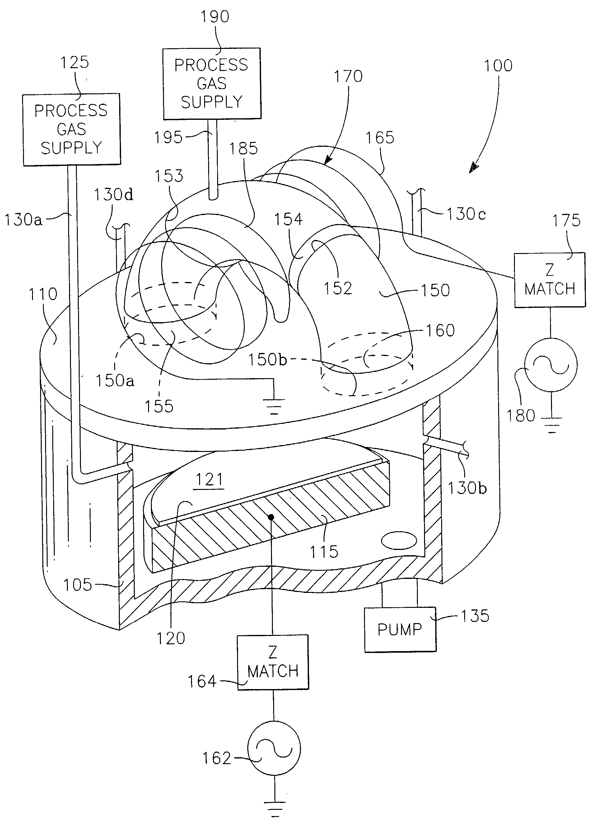
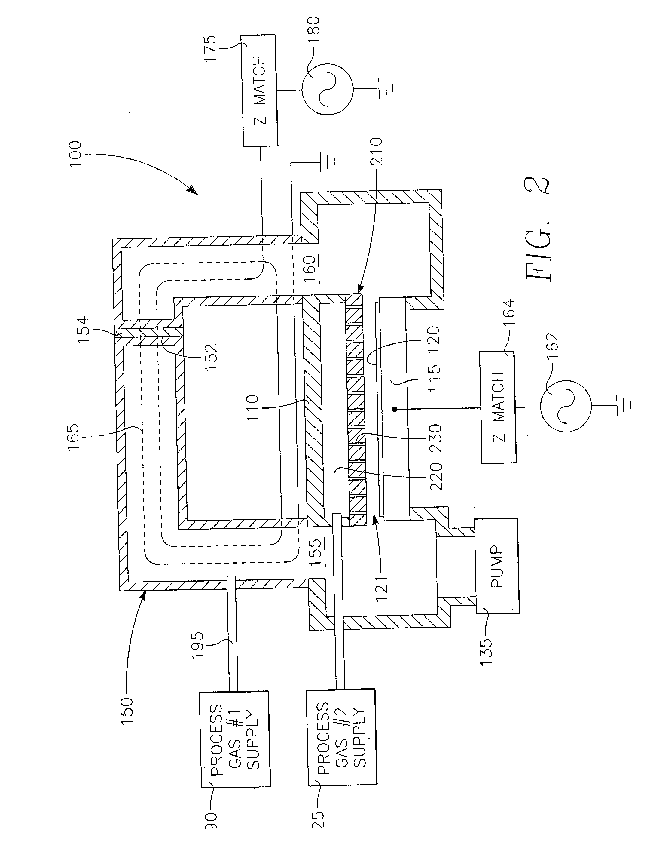
Embodiment Construction

[0204] An etch process was conducted on blanket oxide wafers at a chamber pressure of 40 mT, 4800 watts of 13.56 MHz RF bias power on the wafer pedestal and 1800 Watts of RF source power applied to each reentrant tube 150 at 11.5 MHz and 12.5 MHz, respectively. The magnetic field produced by the electromagnet assembly 4430 was set at the following levels in successive steps: (a) zero, (b) 6 Gauss and (c) 18 Gauss (where the more easily measured axial magnetic field component at the wafer center was observed rather than the more relevant radial component). The observed etch rate distribution on the wafer surface was measured, respectively, as (a) center low with a standard deviation of about 2% at zero Gauss, (b) slightly center fast with a standard deviation of about 1.2% at 6 Gauss, and (c) center fast with a standard deviation of 1.4%. These examples demonstrate the ability to provide nearly ideal compensation (step b) and the power to overcompensate (step c).

[0205] To test the ef...


PUM

PropertyMeasurementUnit
plasma currentaaaaaaaaaa
diameteraaaaaaaaaa

Abstract

A plasma reactor is described that includes a vacuum chamber defined by an enclosure including a side wall and a workpiece support pedestal within the chamber defining a processing region overlying said pedestal. The chamber has at least a first pair of ports near opposing sides of said processing region and a first external reentrant tube is connected at respective ends thereof to the pair of ports. The reactor further includes a process gas injection apparatus (such as a gas distribution plate) and an RF power applicator coupled to the reentrant tube for applying plasma source power to process gases within the tube to produce a reentrant torroidal plasma current through the first tube and across said processing region. A magnet controls radial distribution of plasma ion density in the processing region, the magnet having an elongate pole piece defining a pole piece axis intersecting the processing region.

Description

[0001] 1. Technical Field[0002] The invention concerns plasma reactors used in processing workpieces in the manufacturing of items such as microelectronic circuits, flat panel displays and the like, and in particular plasma sources therefor.[0003] 2. Background Art[0004] The trend in microelectronic circuits toward ever increasing densities and smaller feature sizes continues to make plasma processing of such devices more difficult. For example, the diameter of contact holes has been reduced while the hole depth has increased. During plasma-enhanced etching of a dielectric film on a silicon wafer, for example, the etch selectivity of the dielectric material (e.g. silicon dioxide) to photoresist must be sufficient to allow the etch process to etch a contact hole whose diameter is ten to fifteen times its depth, without appreciably disturbing the photoresist mask defining the hole. This task is made even more difficult because the recent trend toward shorter wavelength light for finer...

Claims


Application Information

Patent Timeline
Patent Type & Authority Applications(United States)
IPC IPC(8): H01J37/32
CPCH01J37/32082H01J37/32412H01J37/321H01J37/00H01J37/32
Inventor COLLINS, KENNETH S.HANAWA, HIROJIYE, YANRAMASWAMY, KARTIKNGUYEN, ANDREWBARNES, MICHAEL S.NGUYEN, HUONG THANH
Owner APPLIED MATERIALS INC
Why Eureka
Try Eureka