
Heteroepitaxial diamond and diamond nuclei precursors

a precursor and diamond technology, applied in the direction of crystal growth process, polycrystalline material growth, condensed vapor, etc., can solve the problem of little agreement on the physical mechanisms that underpin the process, and achieve the effect of enhancing electron emission

Inactive Publication Date: 2004-04-15
BOARD OF TRUSTEES OPERATING MICHIGAN STATE UNIV
View PDF11 Cites 24 Cited by
  • Summary
  • Abstract
  • Description
  • Claims
  • Application Information

AI Technical Summary

Benefits of technology

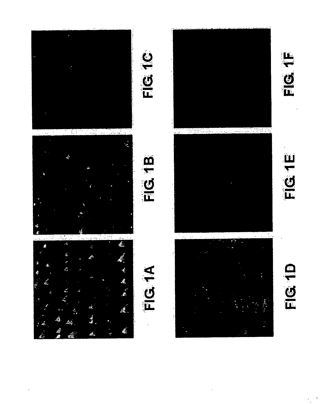
[0039] FIGS. 8A and 8B show scanning electron microscope images of the (001) surface of heteroepitaxial diamond on (001)Ir(001)SrTiO.sub.3 after 60 minutes growth: FIG. 8A substrate center; FIG. 8B substrate edge. Note the slightly incomplete coalescence at the substrate edge in FIG. 8B. The bright spots correspond to enhanced electron emission from small, easily charged diamond topographic features.

Problems solved by technology

Although the conditions that lead to effective nucleation are well known in principle, there is little agreement on the physical mechanisms that underpin the process.

Method used


Image

  • Heteroepitaxial diamond and diamond nuclei precursors
  • Heteroepitaxial diamond and diamond nuclei precursors
  • Heteroepitaxial diamond and diamond nuclei precursors

Examples


example 1

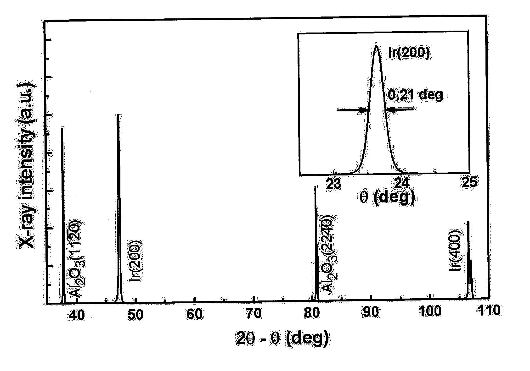
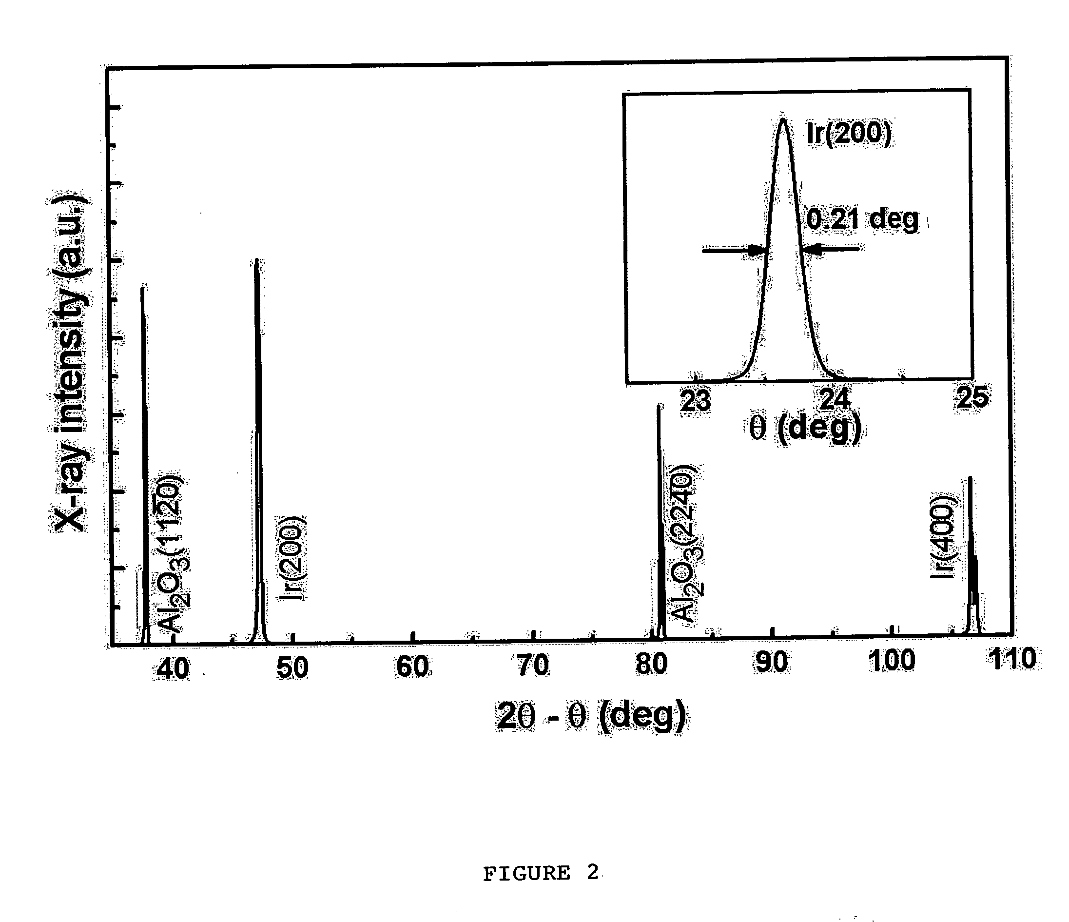
[0072] Single crystal (11-20), or a-plane, sapphire substrates with dimensions 5.times.5.times.0.5 mm.sup.3 were used for epitaxial Ir deposition. The substrates were annealed in a tube furnace to prepare an atomically flat surface. The annealed substrates were then loaded into a UHV chamber, base pressure 10.sup.-10 Torr, via a load-lock and Ir deposition performed by electron-beam evaporation from Ir rods of 99.9% purity. The sapphire substrates were placed in the UHV chamber, heated to 900.degree. C. to 950.degree. C., and Ir deposited at a rate of 2.4 nm / min. The substrate heater was switched off immediately after evaporation and the film allowed to cool to room temperature. After removal from the chamber, the film orientation and crystalline quality were examined by X-ray diffraction (XRD) using CuK.sub..alpha. radiation, and the Gaussian full width at half maximum (FWHM) extracted by a least-squares fit. Film crystallinity and the epitaxial relationship were characterized by E...

example 2

[0082] Substrates and Ir Growth

[0083] All experiments were carried out on 5.times.5.times.0.5 mm.sup.3 substrates obtained from commercial sources. The (001) SrTiO.sub.3 plates were typically cleaned in buffered HF before insertion into a UHV electron-beam evaporator. After in situ annealing for 20 to 120 minutes at 800.degree. C., Ir was deposited at 2.4 nm / minute to a thickness of 150 or 300 nm. No post-deposition annealing was used as it tended to degrade the (001) epitaxial Ir. surface reactions of SrTiO.sub.3 with stainless steel substrate holders were observed. Reduction of the oxide, as evidenced by its darkening, led to a finite electrical conductance across the substrate. Similar behavior was noted for LaAlO.sub.3 but not for MgO.

[0084] Ir growth on polished (11-20) sapphire, or A-plane .alpha.-Al.sub.2O.sub.3 oriented approximately 1.degree. of the a-direction was explored. Substrate preparation consisted of annealing in air at 1450.degree. C. for 15 hr followed by a light...

example 3

[0097] Heteroepitaxial growth of Ir and Ir / diamond on STO (strontium titanate) and A-plane ALO (sapphire) are shown by FIGS. 5 to 23 as discussed above.

[0098] The growth of single crystalline diamond is by heteroepitaxy. Heteroepitaxy is the process of growing a monocrystalline thin or thick film material using as a template a substrate material with substantially the same lattice parameter (the spacing between atoms in the crystal). The process improvements and optimization resulting in diamond of higher crystalline quality, homogeneity, and size are in the following sequential steps:

[0099] 1. Preparation of atomically flat (stepped) lattice-matched single crystal substrates by chemical, physical, and thermal methods. The substrates have surfaces terminated in specified lattice planes. Substrates investigated include sapphire (Al.sub.2O.sub.3), strontium titanate (SrTiO.sub.3), lanthanum aluminate (LaAlO.sub.3), and magnesium oxide (MgO).

[0100] 2. Deposition of epitaxial iridium me...


PUM


Abstract

A process for growing by chemical vapor deposition a heteroepitaxial single crystal diamond is disclosed. The process provides a substrate which enables the growth of single crystal diamond which is vapor coated on an iridium film. An intermediate process for producing a composite composition with diamond nuclei is also described. Further described are composite compositions of metal oxide, iridium and single crystal diamond films or diamond nuclei. Single crystal diamond is useful in a variety of electronics and acoustics fields.

Description

CROSS REFERENCE TO RELATES APPLICATION[0001] This application relies for priority on U.S. provisional application Serial No. 60 / 406,150, filed Aug. 27, 2002.[0003] (1) Field of the Invention[0004] The present invention relates to a process for growing heteroepitaxial single crystal diamond and diamond crystallite precursors. In particular, the present invention uses a surface on a metal oxide substrate coated with a thin film of iridium which enables growing the single crystal diamond or the diamond nuclei as precursors.[0005] (2) Description of Related Art[0006] FCC (face-centered cubic) Ir buffer layers have been used as substrates for single crystal diamond film growth by low pressure chemical vapor deposition (CVD). MgO and SrTiO.sub.3 were used as substrates for (001) Ir films (Ohtsuka, K., et al., Jpn. J. Appl. Phys. 36, 1214 (1997); Schreck, M., et al., Appl. Phys. Lett. 74 650 (1999); and Tsubota, T., et al., Diamond and Related Materials 9 1380 (2000)). Cubic MgO (Ohtsuka, ...

Claims


Application Information

Patent Timeline
IPC IPC(8): C30B25/10
CPCC30B25/105C30B29/04
Inventor GOLDING, BRAGEBEDNARSKI-MEINKE, CONNIEDAI, ZHONG-NING
Owner BOARD OF TRUSTEES OPERATING MICHIGAN STATE UNIV
Learn More