

Optical device structures based on photo-definable polymerizable composites
a composite material and optical device technology, applied in the field of optical device structures comprising polymeric composite materials, can solve the problems of difficult fabrication of mirrors using conventional methods, light transmission losses, waveguide structures, etc., and achieve excellent heat sink properties and high surface quality
- Summary
- Abstract
- Description
- Claims
- Application Information
AI Technical Summary
Benefits of technology
Problems solved by technology
Method used
Image

Examples
Embodiment Construction
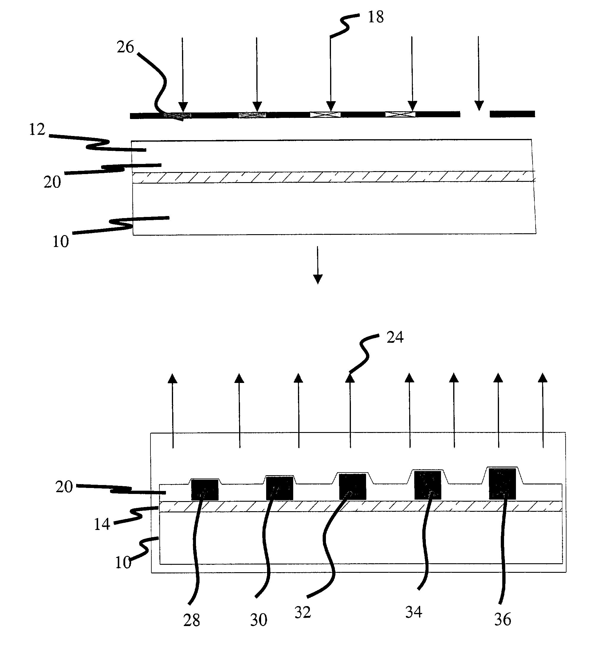
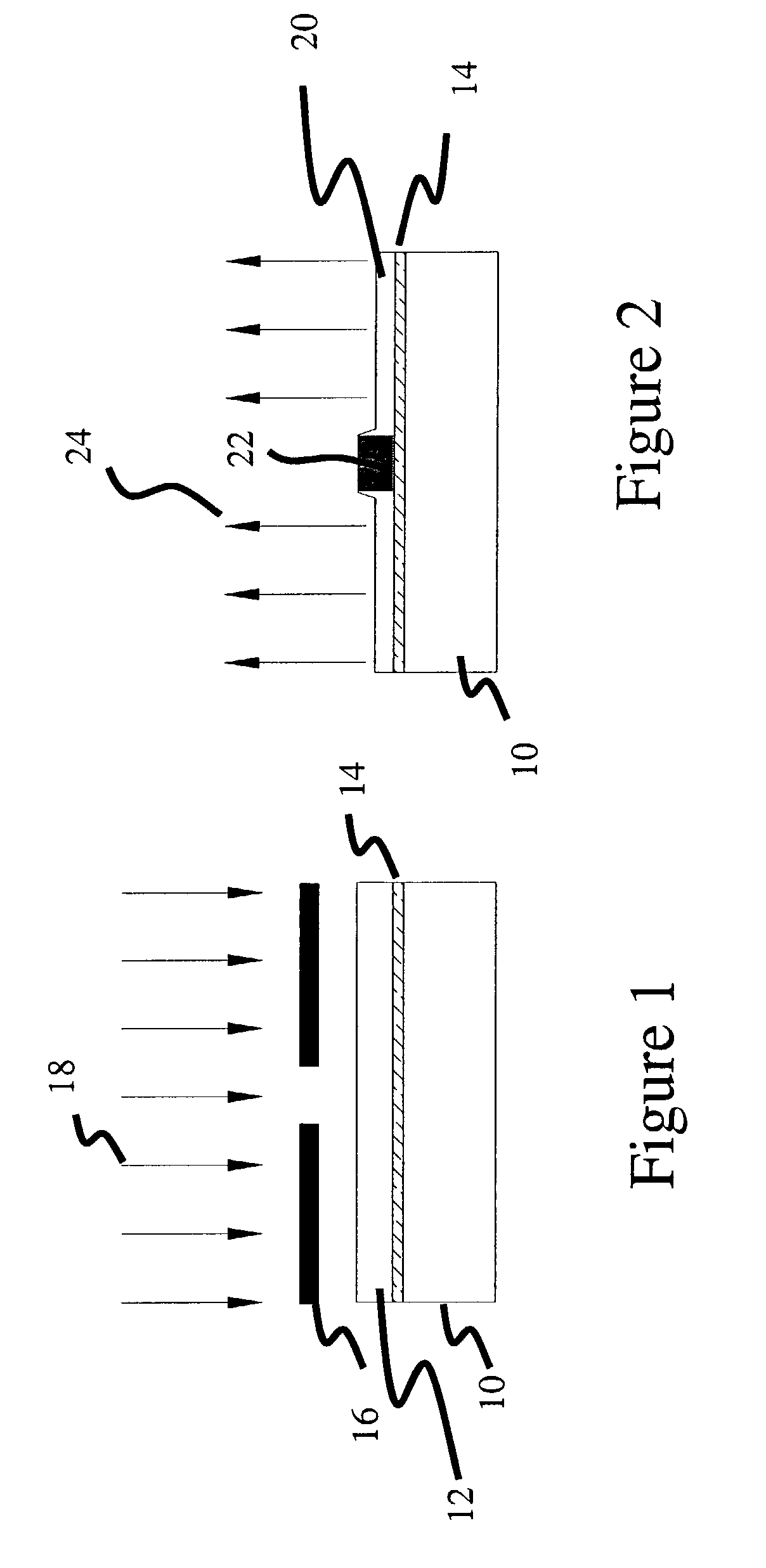
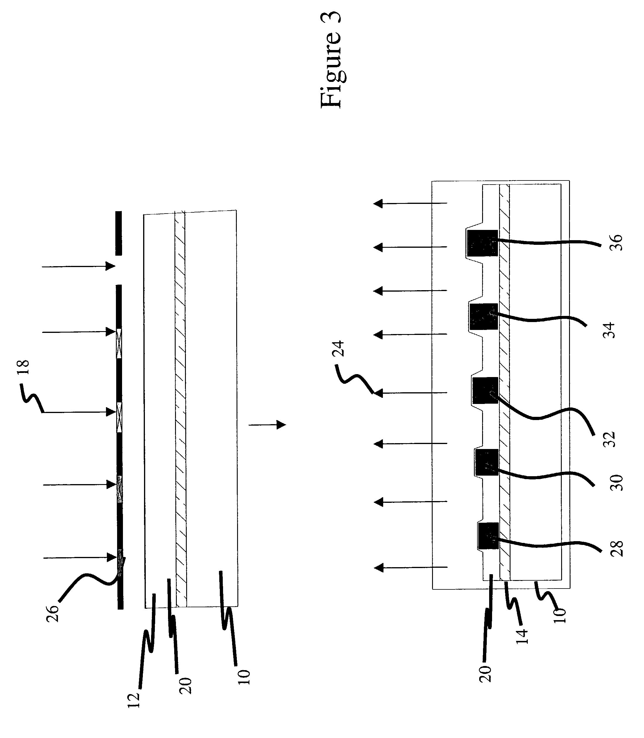
[0047] This Example describes the preparation of a surface topography comprising a polymeric composite material derived from Apec.TM. 9371 polycarbonate (available from Bayer Company) and CY 179 using UV-irradiation.
[0048] A mixture was prepared containing approximately 50 parts by weight Apec.TM. polycarbonate, approximately 50 parts by weight of CY 179, 1 part by weight of Cyracure UVI-6976 photo catalyst, 150 parts by weight anisole and 50 parts by weight cyclopentanone. A 50 micron thick film was prepared on a glass substrate by spin coating the material and partially curing it for 20 minutes at 90.degree. C. to remove the solvent. A patterned chrome image on a quartz plate was used to expose and define a pattern on the polycarbonate / epoxy film. A 30 second exposure using a Karl Suss contact printer was used. After exposure, the sample was baked on a hotplate for 1 hour at 200.degree. C. Surface profilometry measurements of the resulting surface topography indicated approximatel...
PUM
 Abstract
Description
Claims
Application Information