

Nickel-coated free-standing silicon carbide structure for sensing fluoro or halogen species in semiconductor processing systems, and processes of making and using same
a technology of silicon carbide and which is applied in the field of devices and methods for sensing fluoro or halogen species, can solve the problems of reducing tool life, long process cycles, and unnecessary global warming gas loss to the atmospher
- Summary
- Abstract
- Description
- Claims
- Application Information
AI Technical Summary
Benefits of technology
Problems solved by technology
Method used
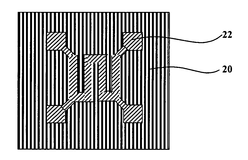
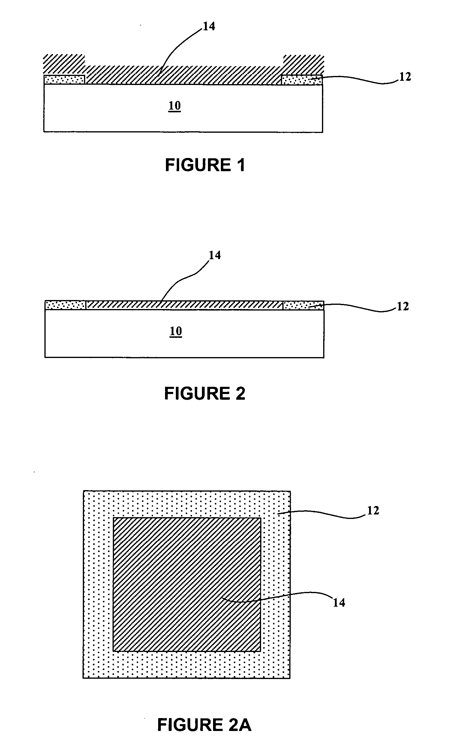
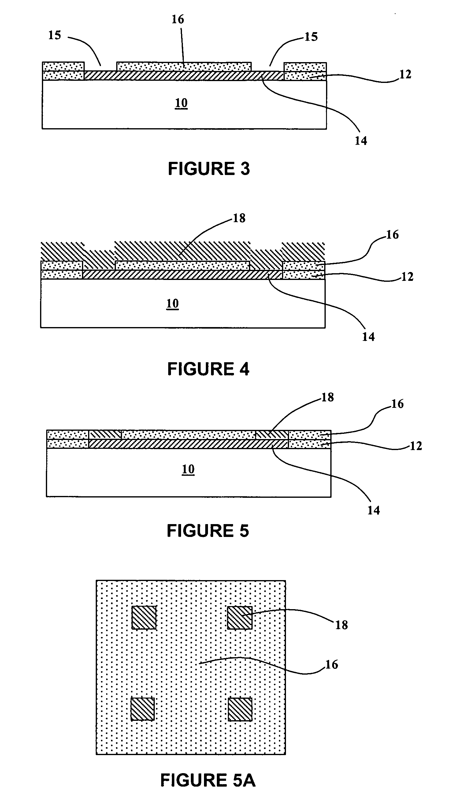
Image

Examples
Embodiment Construction
[0077] The contents of U.S. patent application Ser. No. 10 / 273,036 filed Oct. 17, 2002 for "APPARATUS AND PROCESS FOR SENSING FLUORO SPECIES IN SEMICONDUCTOR PROCESSING SYSTEMS" and U.S. Pat. No. 6,265,222 issued Jul. 24, 2001 for "MICRO-MACHINED THIN FILM HYDROGEN GAS SENSOR, AND METHOD OF MAKING AND USING THE SAME" are incorporated herein by reference in their entirety for all purposes.
[0078] While the invention is described more fully hereinafter with specific reference to applications in semiconductor process control, it is to be appreciated that the utility of the invention is not thus limited, but rather extends to a wide variety of other uses and applications, including, without limitation, deployment in life safety systems, room or ambient environment monitoring operations, and other industrial as well as consumer market gas sensing applications.
[0079] The present invention in one aspect thereof provides microelectromechanical system (MEMS)-based gas sensing capability for d...
PUM
 Abstract
Description
Claims
Application Information