Nitride semiconductor laser device and method of manufacturing the nitride semiconductor laser device

a laser device and semiconductor technology, applied in the direction of lasers, semiconductor laser structure details, semiconductor lasers, etc., can solve the problems of poor lifetime thought to be caused, many defects may occur in the wafer of the laser device described, poor reproducibility upon cleavage, etc., to prevent the occurrence of chipping and the like, good lifetime, and high reliability

Active Publication Date: 2005-02-10
NICHIA CORP
View PDF3 Cites 26 Cited by
  • Summary
  • Abstract
  • Description
  • Claims
  • Application Information

AI Technical Summary

Benefits of technology

[0008] An object of the present invention is to provide a nitride semiconductor laser device having good lifetime with high r

Problems solved by technology

However, many defects may occur in a wafer of the laser device described above, such as poor reproducibility upon cleavage or a poor lifetime thought to be caused by deterioration due to insufficient heat dissipation.
There have been other problems with the construction of the nitride semiconductor laser device.
These problems include that the width of the ridge is small compared with the chip size of the nitride semiconductor laser device so that the damage tends to concentrate in the ridge.
Also, the deteri

Method used


Image

  • Nitride semiconductor laser device and method of manufacturing the nitride semiconductor laser device
  • Nitride semiconductor laser device and method of manufacturing the nitride semiconductor laser device
  • Nitride semiconductor laser device and method of manufacturing the nitride semiconductor laser device

Examples


embodiments 1 and 2

[0054] (First Process)

[0055] First, a nitride semiconductor substrate 101 is prepared (FIG. 7A). A nitride semiconductor is grown on a foreign substrate such as sapphire or GaAs via a buffer layer (not shown). After that, the foreign substrate is removed by grinding, electromagnetic irradiation (excimer laser radiation etc.), or CMP, etc. and the nitride semiconductor substrate 101 is obtained. A surface having n-polarity is exposed on the nitride semiconductor where the foreign substrate was removed. A damaged layer may appear on the n-polarity surface as a result of removing the foreign substrate by grinding or excimer laser irradiation, the damaged layer can be removed by CMP or dry etching. By this process, the thickness and the surface roughness of the nitride semiconductor can also be adjusted by removing the damaged layer. The resulting nitride semiconductor substrate 101 comprises a first main surface and a second main surface with a thickness from 0.2 mm to 10 mm.

[0056] T...

embodiment 3

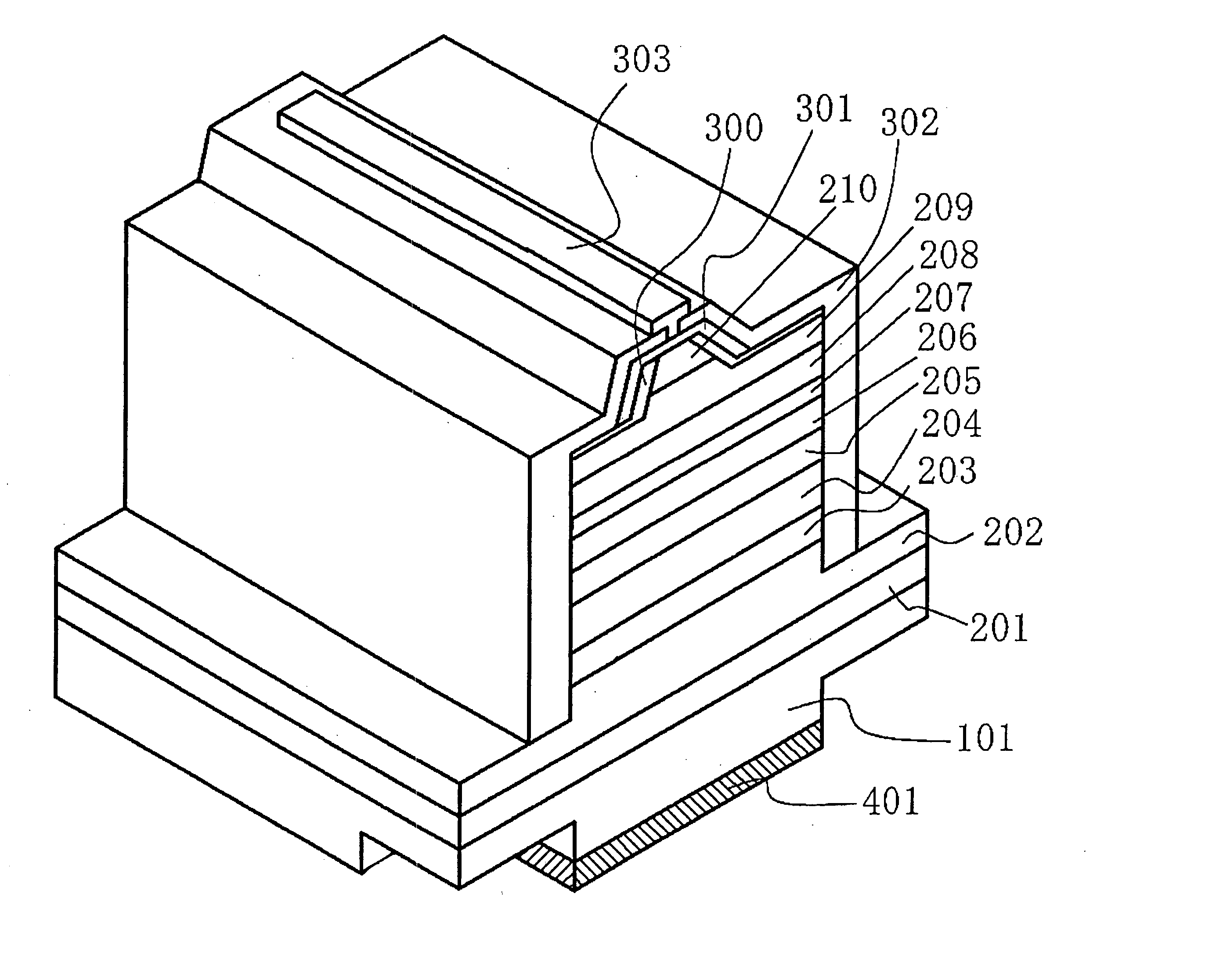
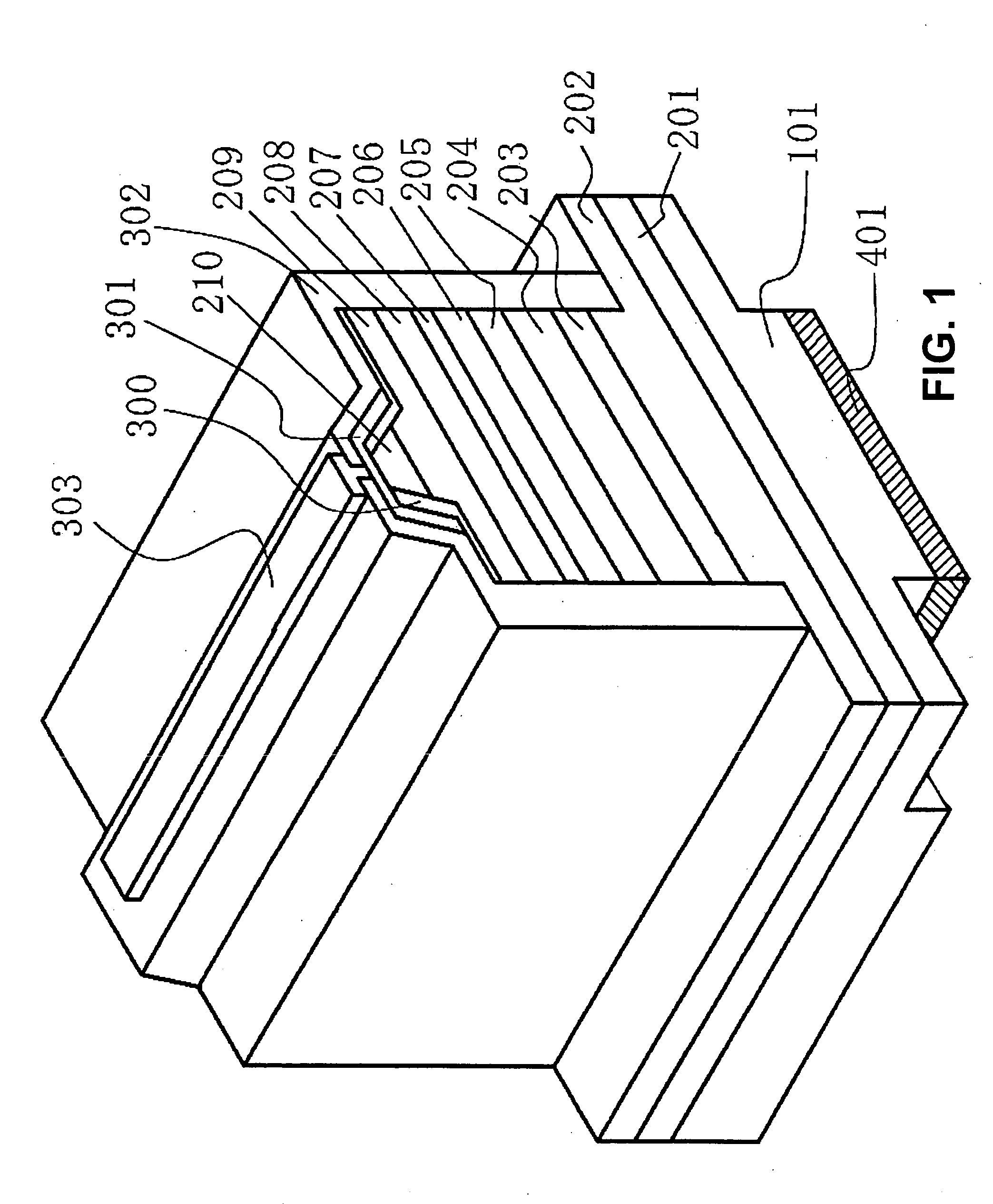
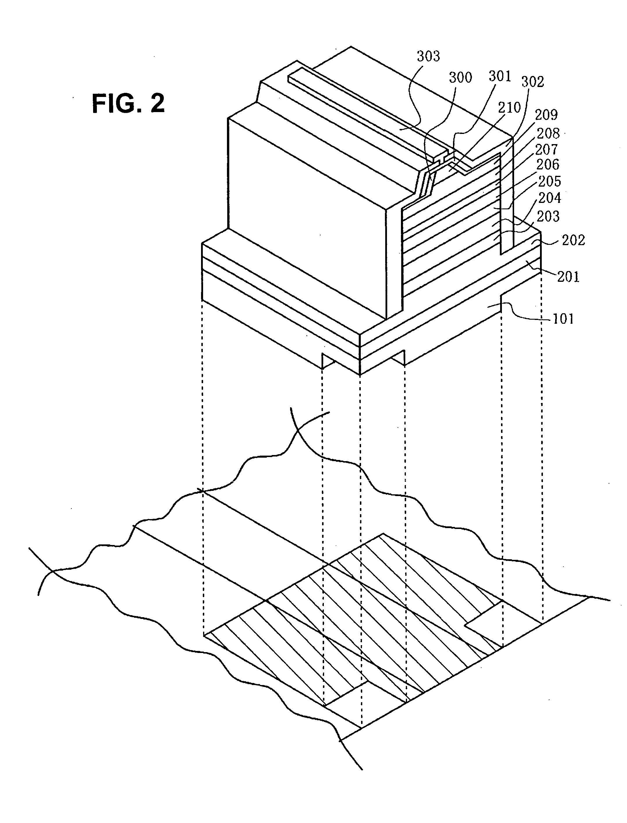
[0082] The nitride semiconductor device may have a structure which includes a current blocking layer. After forming the n-side contact layer 202, the crack preventing layer 203, the n-side cladding layer 204, and the n-side optical guide layer 205 are formed on the nitride semiconductor 1. The current blocking layer is then formed with a stripe-shaped opening with a width of from 0.5 to 3.0 μm and a thickness of 3,000 Å or less. Next, the active layer having a quantum well structure 206 is formed on the n-side optical guide layer which is exposed at the opening of the current blocking layer. Then, the p-side electron confinement layer 207, the p-side optical guide layer 208, the p-side cladding layer 209, and the p-side contact layer 210 are formed. The current blocking layer can be made of an i-type or intrinsic nitride semiconductor or other insulating materials such as SiO2, or Al2O3.

[0083] The current blocking layer is not limited to being formed after growing the n-side optica...

example 1

[0085] A foreign substrate made of sapphire having a C-plane as a main surface is set in the MOVPE reactor vessel. The temperature is adjusted to 500° C. and a buffer layer made of GaN is grown to a the thickness of 200 angstroms, using trimethylgallium (TMG) and ammonia (NH3). After growing the buffer layer, the temperature is adjusted to 1050° C. and an underlayer made of GaN is grown to a thickness of 4 μm. A protective layer is partially formed on the underlayer in preparation for selective growth of the nitride semiconductor.

[0086] After the underlayer is grown, the wafer is taken out from the reactor vessel and a stripe-shaped photomask is disposed on the surface of the underlayer. Then, a protective layer of SiO2 is formed with a stripe width from 10 to 300 μm and a stripe interval (window portion) from 5 to 300 μm.

[0087] (Nitride Semiconductor Substrate)

[0088] After forming the protective layer, the wafer is once again set in the reactor vessel of MOVPE. The temperature i...


PUM


Abstract

The nitride semiconductor laser device has a counter electrode structure where contact resistance is reduced and manufacturing methods thereof are provided. The nitride semiconductor laser device comprises a nitride semiconductor substrate having a first main surface and a second main surface. A nitride semiconductor layer is stacked on the first main surface of the nitride semiconductor substrate. A ridge-shaped stripe is formed in the nitride semiconductor layer, and a resonance surface forms an optical waveguide in the direction perpendicular to the length of the ridge-shaped stripe. A first region having a crystal growth facet in the (0001) plane and a second region on the first main surface or the second main surface are provided. Further, a recess is formed in the second region of the first main surface and/or the second main surface. A ridge-shape stripe is formed over the first main surface of the nitride semiconductor substrate.

Description

BACKGROUND OF THE INVENTION [0001] 1. Field of the Invention [0002] The present invention relates to a nitride semiconductor laser made of a nitride semiconductor (InaAlbGa1-a-bN, 0≦a, 0≦b, a+b≦1), and particularly to a nitride semiconductor laser device formed with a good resonant surface that is reproducible by way of a cleavage process and has an excellent lifetime and mass productivity. [0003] 2. Discussion of the Related Art [0004] Recently, small size, lightweight, high reliability, and a high output properties have been required for nitride semiconductor laser devices, and they are used as a light source for an optical disc such as a DVD and a light source for medical equipment. Various research has been conducted on nitride semiconductor laser devices. [0005] For example, as a practical laser device, a nitride semiconductor laser device capable of continuous-wave oscillation of more than 10,000 hours at room temperature is described in Japan Journal of Applied Physics, Vol. ...

Claims


Application Information

Patent Timeline
IPC IPC(8): H01S5/02H01S5/30H01S5/22H01S5/32H01S5/323H01S5/343
CPCB82Y20/00H01S5/0201H01S5/0202H01S2304/12H01S5/3202H01S5/32341H01S5/34333H01S5/2214H01S5/320225H01S5/04254H01S5/30
Inventor KOZAKI, TOKUYASAKAMOTO, KEIJIMATSUMURA, HIROAKI
Owner NICHIA CORP
Why Eureka
Try Eureka