Stress-controlled dielectric integrated circuit

a dielectric integrated circuit and stress-controlled technology, applied in the direction of instruments, photomechanical equipment, and semiconductor/solid-state device details, can solve the problems of significant number and complexity of processing steps presently used, and achieve the effects of reducing processing complexity, reducing processing costs, and reducing device isolation processing steps

Inactive Publication Date: 2005-03-10
TAIWAN SEMICON MFG CO LTD
View PDF69 Cites 25 Cited by
  • Summary
  • Abstract
  • Description
  • Claims
  • Application Information

AI Technical Summary

Benefits of technology

The benefits to fabricating an IC with the MDI process are significant over prior art methods, some of these benefits being: 1. Complete electrical isolation of semiconductor devices. 2. Vertical semiconductor device structures. 3. Lower processing costs through lower processing complexity or fewer device isolation processing steps. 4. Conformal mask lithography through the membrane substrate. 5. Control of depth of focus during lithography exposure due to control of substrate thickness. 6. Applicatio...

Problems solved by technology

ICs formed from dielectric and semiconductor membranes can reduce significantly the number and complexity of processing steps presently used to provide complete IC device isolation; die...

Method used


Image

  • Stress-controlled dielectric integrated circuit
  • Stress-controlled dielectric integrated circuit
  • Stress-controlled dielectric integrated circuit

Examples


Embodiment Construction

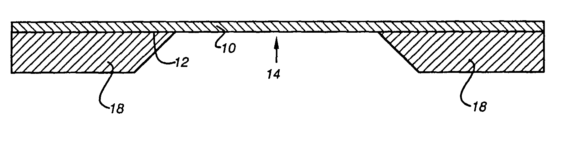
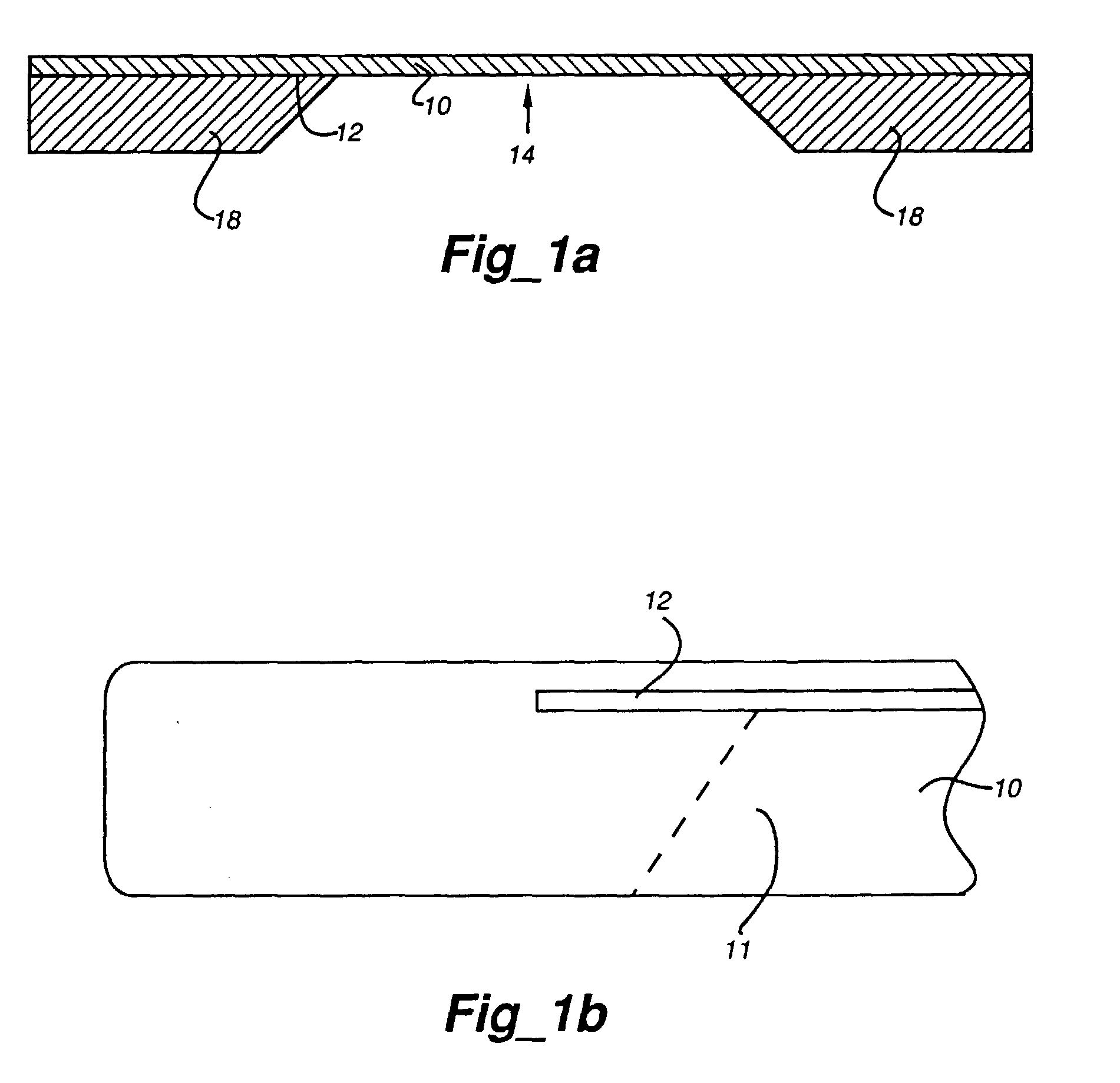
The MDI process is the formation of an IC or interconnect metallization circuit as a free standing dielectric and / or semiconductor circuit membrane. Each semiconductor device comprising an IC circuit membrane is a semiconductor device optionally isolated from adjoining semiconductor devices, and where each semiconductor device is formed on or in a membrane of semiconductor material typically less than 8 μm in thickness. The overall thickness of a circuit membrane is typically less than 50 μm and preferably less than 8 μm. The dielectric membrane is compatible with most higher temperature IC processing techniques.

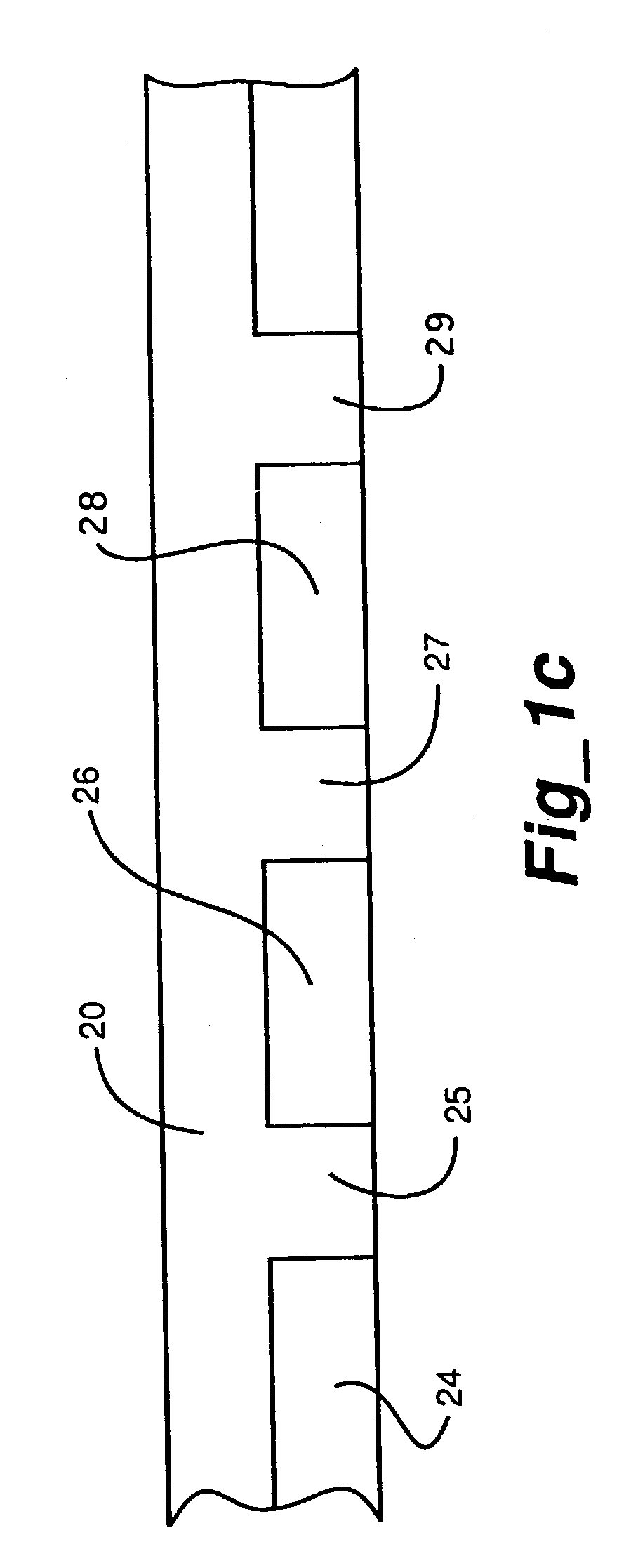
MDI Fabrication Process

Several process variations can be used to form the thin film or membrane of semiconductor material for use in the MDI process. Additional related methods for forming semiconductor membranes may exist or come into existence and are included in the MDI technology.

Examples of some of the methods that can be used for forming silicon single crystal t...


PUM

PropertyMeasurementUnit
Temperatureaaaaaaaaaa
Lengthaaaaaaaaaa
Thicknessaaaaaaaaaa

Abstract

General purpose methods for the fabrication of integrated circuits from flexible membranes formed of very thin low stress dielectric materials, such as silicon dioxide or silicon nitride, and semiconductor layers. Semiconductor devices are formed in a semiconductor layer of the membrane. The semiconductor membrane layer is initially formed from a substrate of standard thickness, and all but a thin surface layer of the substrate is then etched or polished away. In another version, the flexible membrane is used as support and electrical interconnect for conventional integrated circuit die bonded thereto, with the interconnect formed in multiple layers in the membrane. Multiple die can be connected to one such membrane, which is then packaged as a multi-chip module. Other applications are based on (circuit) membrane processing for bipolar and MOSFET transistor fabrication, low impedance conductor interconnecting fabrication, flat panel displays, maskless (direct write) lithography, and 3D IC fabrication.

Description

BACKGROUND OF THE INVENTION 1. Field of the Invention This invention relates to methods for fabricating integrated circuits on and in flexible membranes, and to structures fabricated using such methods. 2. Description of Related Art Mechanically and thermally durable free standing dielectric and semiconductor membranes have been disclosed with thicknesses of less than 2 μm. (See commonly invented U.S. Pat. No. 4,924,589, and U.S. patent application Ser. No. 07 / 482,135, filed Feb. 16, 1990, now U.S. Pat. No. 5,103,557, both incorporated herein by reference). This disclosure combines the novel use of these technologies and other integrated circuit (IC) processing techniques to form ICs as membranes typically less than 8 μm thick. This approach to IC fabrication falls under the generic industry-established title known as Dielectric Isolation (DI), and is inclusive of subject areas such as Silicon-on-Insulator (SOI) and Silicon-on-Sapphire (SOS). ICs formed from dielectric and semic...

Claims


Application Information

Patent Timeline
IPC IPC(8): G21K5/02B81B3/00G02F1/13G03F7/20G11C29/00H01L21/027H01L21/306H01L21/331H01L21/336H01L21/76H01L21/762H01L21/764H01L21/822H01L21/8234H01L21/8238H01L21/98H01L23/48H01L23/538H01L25/065H01L27/00H01L27/02H01L27/08H01L27/088H01L27/092H01L27/12H01L29/732H01L29/78H01L29/786H05G1/00
CPCG02F1/13452H01L2924/0002G03F7/70658G11C29/006H01L21/762H01L21/76264H01L21/76289H01L21/764H01L21/8221H01L23/481H01L23/538H01L23/5381H01L23/5383H01L23/5386H01L23/5387H01L25/0652H01L25/0655H01L25/50H01L27/0207H01L2224/0557H01L2224/13009H01L2224/16H01L2924/01014H01L2924/0102H01L2924/01057H01L2924/01078H01L2924/01079H01L2924/13091H01L2924/14H01L2924/15153H01L2924/15165H01L2924/15312H01L2924/3011H01L2924/3025H01L2924/01019Y10S438/938Y10S438/928Y10S148/135Y10S438/977Y10S438/942Y10S438/967G02F2001/136281H01L2924/1305Y10T29/49165Y10T29/4921H01L2224/0401Y10T29/49128Y10T29/49171Y10T29/49162H01L2924/00H01L2224/05552G02F1/136281H01L2224/16225H01L2224/16227H01L2924/00011H01L2224/80001H01L21/00
Inventor LEEDY, GLENN JOSEPH
Owner TAIWAN SEMICON MFG CO LTD
Why Eureka
Try Eureka