Light emitting apparatus

a technology of light-emitting apparatus and light-emitting gan, which is applied in the direction of electrical apparatus, basic electric elements, and semiconductor devices, can solve the problems of unavoidably increasing the fabrication cast, complicated construction, and significant complexity of the gan-based led construction, and achieves simple construction, high light-emitting efficiency, and easy fabrication.

Active Publication Date: 2005-03-24
SUMITOMO ELECTRIC IND LTD
View PDF9 Cites 39 Cited by
  • Summary
  • Abstract
  • Description
  • Claims
  • Application Information

AI Technical Summary

Benefits of technology

[0017] It is an object of the present invention to provide light emitting apparatuses which have simple constructions and thus can be fabricated easily, and can stably provide high light emission efficiencies for a long time period.
[0020] Further, the p-type nitride semiconductor layer side having a high electrical resistance does not form a light emitting surface and therefore the p-type electrode layer may be formed on the entire surface of the p-type nitride semiconductor layer. This construction is advantageous in flowing large currents and suppressing heat generation and in discharging generated heat by conduction. Namely, restrictions caused by heat requirements may be drastically alleviated. Thus, there is no need to form a comb-shaped electrode in which the n-electrode and the p-electrode are complicated in order to reduce the electrical resistance.
[0021] Since the GaN substrate has an excellent conductivity, there is no need to provide a protection circuit against surge voltages and the breakdown strength may be made significantly higher.
[0022] Further, complicated process steps are not performed and the fabrication cost may be easily reduced.
[0025] This construction is predicated on that the above GaN substrate of the present invention has a conductivity and the electrical resistance may be easily reduced. In addition to the effects of the aforementioned light emitting apparatus, since the GaN substrate has a dislocation density of 108 / cm2 or less and the crystalinity is high and also the opening ratio is high, the light output from the second main surface may be increased. Further, light is emitted from the side surfaces.
[0028] AlN has a significantly high heat conductivity and thus is excellent in heat dissipation ability. Therefore, it is possible to suppress temperature increases in the light emitting apparatus by transferring heat from the above p-type AlxGa1-xN layer to the lead frame, etc. Further, the above AlN substrate also dissipates heat, which contributes to suppression of temperature increases. Further, this construction is predicated on that the AlN substrate is a conductive AlN substrate into which impurities have been implanted to provide a conductivity.

Problems solved by technology

The construction of the GaN-based LED is significantly complicated as can be seen in FIG. 59.
In the case of GaN-based LEDs using a sapphire substrate illustrated in FIG. 59, the construction is complicated and the fabrication cast will be unavoidably increased.
In order to develop the demand in large space illumination applications, LEDs are required to be cheap, and thus the aforementioned construction is not desirable.
However, with the construction illustrated in FIG. 59, the area of the p-electrode is restricted and accordingly the light output is restricted.
Further, in discharging heat generated in association with currents, providing two electrodes on one side is not desirable.
Furthermore, there is large resistance to currents flowing in the direction parallel to the substrate through n-type GaN layer 102, which causes heat generation and an increase of the driving voltage and, therefore, an increase of the power consumption.
Particularly, if the thickness of the n-type GaN layer is reduced in order to shorten the film forming processes, the yield of exposure of the n-type GaN film will be significantly degraded, besides the above problem of heat generation and power consumption increases.
Further, as can be said in general for light emitting devices including the above light emitting device employing a sapphire substrate, since the heat radiating area is restricted and also the heat resistance (temperature increase caused by unit introduced energy per unit area) is large, the injection current per light emitting apparatus can not be increased.
Further, in the case of GaN-based LEDs using a sapphire substrate, since the heat radiating area is restricted, in order to reduce the electrical resistance as much as possible to reduce heat generation, it becomes necessary to employ a construction in which the p-electrode and the n-electrode are complicated in a comb shape to widen the contact area.
Processing of such a comb-shaped electrode is not easy and the fabrication cost will be certainly increased.
Further, there are the following problems.
Although the problem of the light emission efficiency is important, there are still other problems.
The sealing resin placed at the side portions of the GaN layers and irradiated with the light is damaged and this causes a problem of shortening the life of the light emitting apparatus.
In the case of a GaN-based LED having a construction of (SiC substrate backside n-electrode / SiC substrate / n-type GaN layer / quantum-well laminate construction (light emitting layer) / p-type GaN layer / p-electrode) for extracting light from the p-layers side, the light absorption ratio at the p-electrode is large and thus high light outputs can not be emitted to the outside efficiently.
Consequently, light emission can not be activated through the entire quantum-well construction, and thus the light emission output is decreased.
Further, the electrical resistance will be increased and this will induce a problem of heat generation and power supply capacity.

Method used


Image

  • Light emitting apparatus
  • Light emitting apparatus
  • Light emitting apparatus

Examples


example c

INVENTIVE EXAMPLE C

[0127] (c1) to (c5) The same processes as the corresponding processes of Inventive Example A were performed, but a larger GaN substrate was employed.

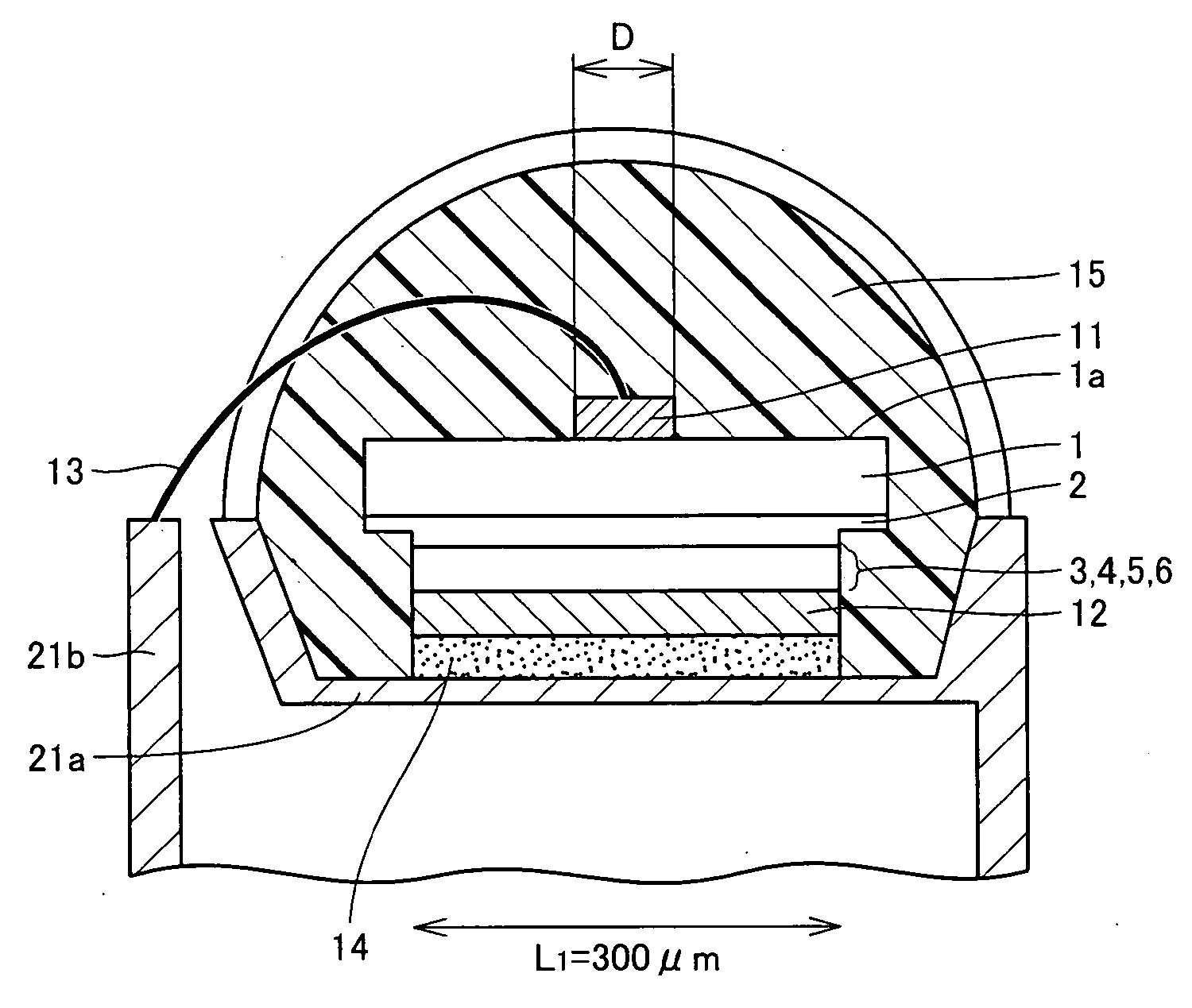
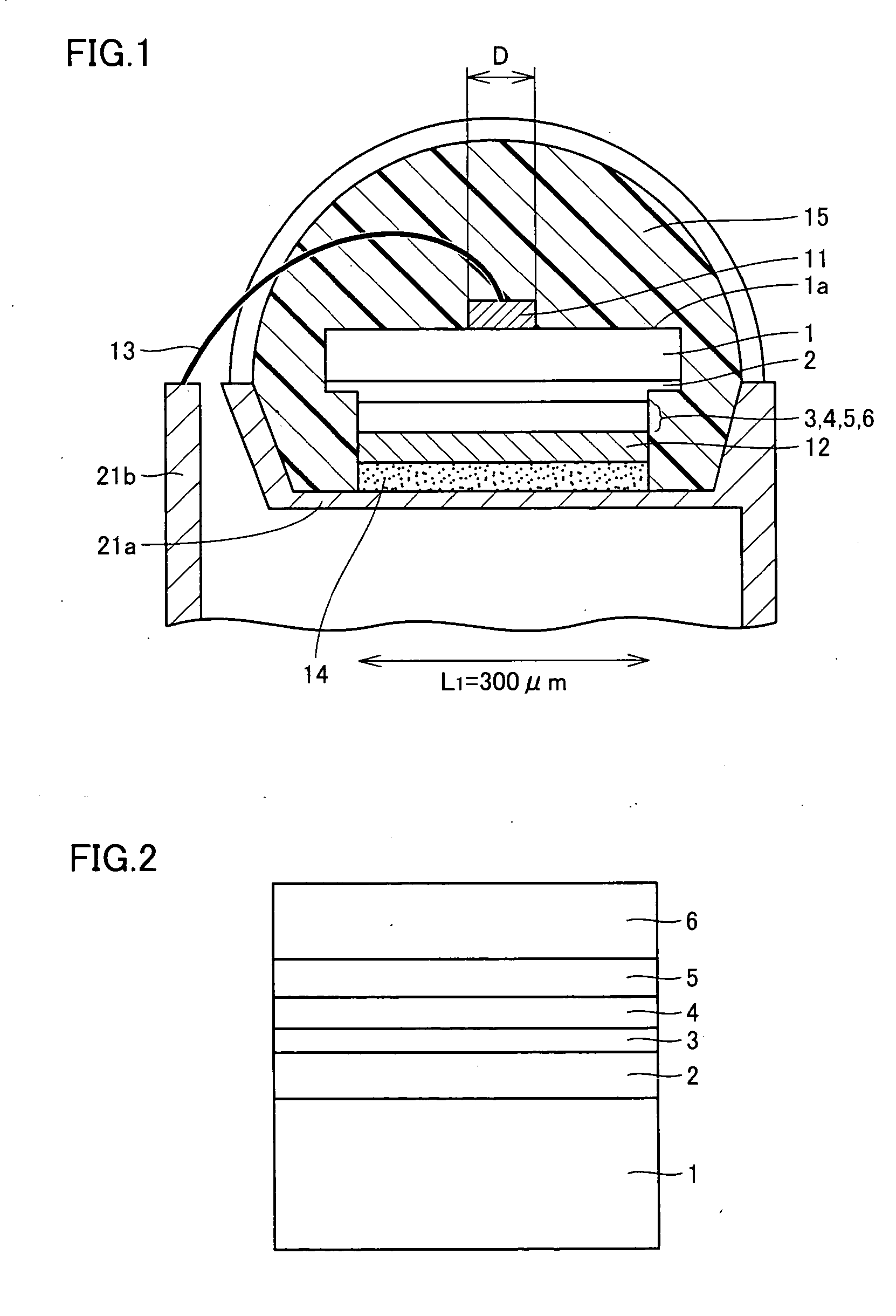
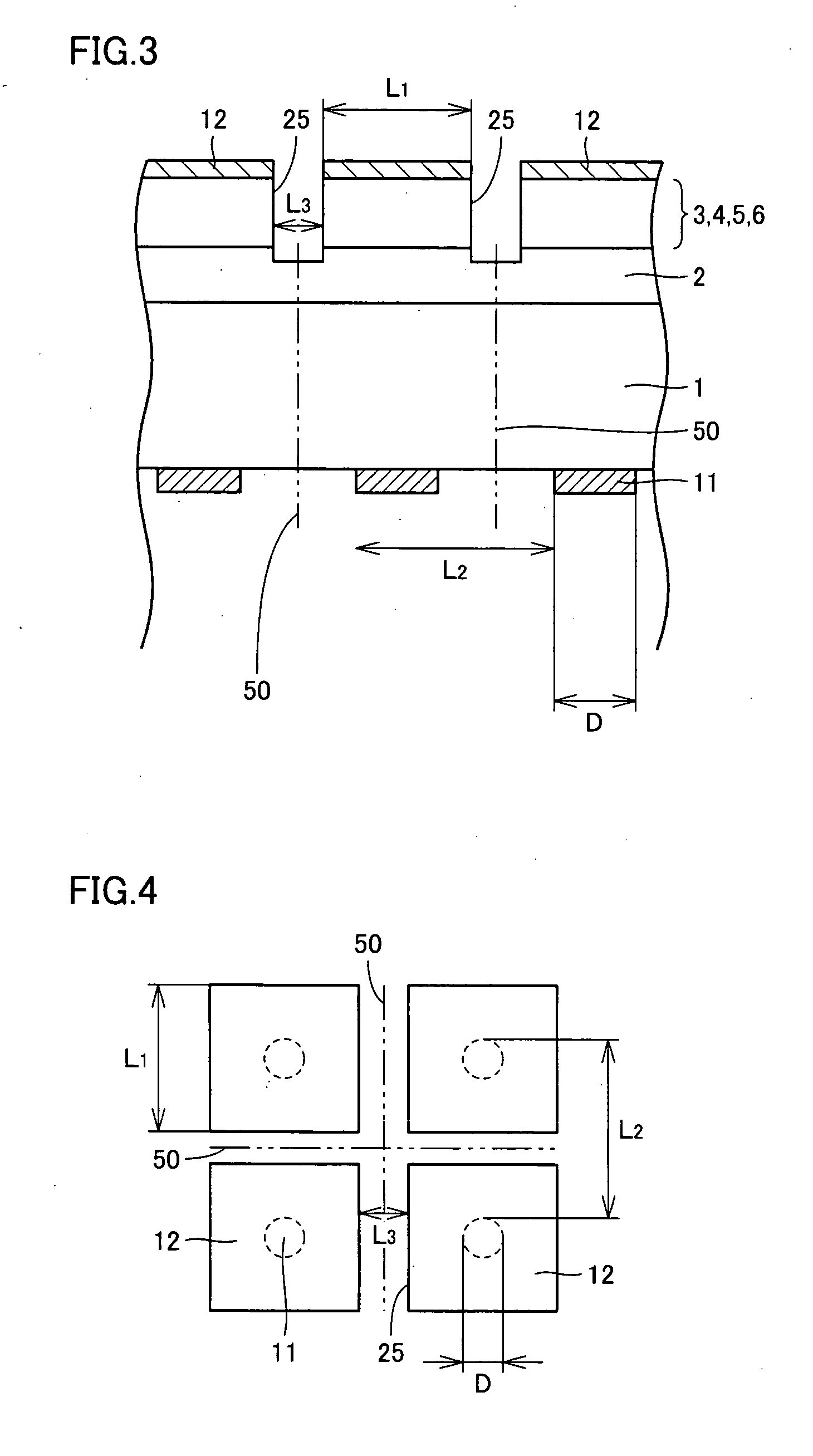
[0128] (c6) On the second main surface at the back side of the GaN substrate, n-electrodes with a diameter of 100 μm are formed with a pitch of 3.1 mm by a photolithography technique, vapor deposition and lift-off method. As the n electrodes, a laminate construction consisting, from the bottom side, of (a Ti layer 20 nm / an Al layer 100 nm / a Ti layer 20 nm / an Au layer 200 nm) was formed in contact with the back side of the above GaN substrate. This was heated in an inert atmosphere to reduce the contact resistance to below 1E-5 Ω·cm2.

[0129] (c7) The same process as the corresponding process of Inventive Example A was performed.

[0130] (c8) Subsequently, the construction was scribed to make it to be desired shapes and the chipped constructions were made to be light emitting devices. The chipped light emitting devices ...

example f

INVENTIVE EXAMPLE F

[0153] (f1) to (f5) The same processes as the corresponding processes of Inventive Example A were performed.

[0154] (f6) Subsequently, as illustrated in FIG. 17, the construction was scribed to be desired shapes and the chip-shaped constructions formed light emitting devices. The resultant light emitting devices had a size of 8 mm square.

[0155] (f7) to (f11) The same processes as the corresponding processes of Inventive Example A were performed.

[0156] (f12) In addition to the above (f11), a white-emitting lamp was fabricated by mounting a fluorescence material on the n-electrode side of the light emitting device which had been mounted on the mount of the lead frame in (f10) and then sealing the light emitting device with an epoxy resin. For this, a fluorescence material which generated 180 lm for 1 watt of light output with 450 nm was employed.

COMPARATIVE EXAMPLE G

[0157] (g1) An n-type GaN off-substrate angled by 0.5° with respect to the c-plane was employed. ...

example i

INVENTIVE EXAMPLE I

[0181] (i1) An n-type GaN off-substrate angled by 0.5° with respect to the c-plane was employed. This GaN substrate had a resistivity of 0.01 Ω·cm and a dislocation density of 1E7 / cm2. This GaN substrate had a thickness of 100 μm.

[0182] (i2) The following layers were formed in order on the first main surface of the GaN substrate by MOCVD. Namely, a laminate construction (a GaN buffer layer / a Si-doped n-type GaN layer / a Si-doped n-type Al0.2Ga0.8N layer being a clad layer / a MQW layer consisting of three layers each being a two-layers construction comprised of a GaN layer and an In0.05Ga0.95N layer / a Mg-doped p-type Al0.2Ga0.8N layer being a clad layer / a Mg-doped p-type GaN layer) was formed.

[0183] (i3) The light emission wavelength was 380 nm. The internal quantum efficiency was 50%, which was calculated for convenience by comparing the PL intensity at a low temperature of 4.2 K and the PL intensity at a room temperature of 298 K.

[0184] (i4) to (i5) The same pro...


PUM


Abstract

In order to provide light emitting devices which have simple constructions and thus can be fabricated easily, and can stably provide high light emission efficiencies for a long time period, a light emitting device includes an n-type nitride semiconductor layer at a first main surface side of a nitride semiconductor substrate, a p-type nitride semiconductor layer placed more distantly from the nitride semiconductor substrate than the n-type nitride semiconductor layer at the first main surface side and a light emitting layer placed between the n-type nitride semiconductor layer and the p-type nitride semiconductor layer at the first main surface side. The nitride semiconductor substrate has a resistivity of 0.5 Ω·cm or less and the p-type nitride semiconductor layer side is down-mounted so that light is emitted from the second main surface of the nitride semiconductor substrate at the opposite side from the first main surface.

Description

BACKGROUND OF THE INVENTION [0001] 1. Field of the Invention [0002] The present invention relates to light emitting apparatuses and more particularly to light emitting apparatuses formed from nitride semiconductors. A light emitting apparatus of the present invention refers to a semiconductor device or semiconductor chip mainly constituted by a nitride semiconductor substrate and semiconductor layers laminated thereon in some cases and also refers to a device including a semiconductor chip mounted on a mounting component and sealed with resin in some cases. Also, it may refer to the both in some cases. Further, a semiconductor chip is called a chip in some cases. Further, a substrate and epitaxial layers formed thereon in a chip are simply called a substrate in some cases. [0003] 2. Description of the Background Art [0004] Currently, white light emitting diodes (LEDs) have been widely employed for illumination of compact electronic equipment such as portable information terminals an...

Claims


Application Information

Patent Timeline
Patent Type & Authority Applications(United States)
IPC IPC(8): H01L29/24H01L33/06H01L33/12H01L33/32H01L33/40H01L33/50H01L33/54H01L33/56H01L33/60H01L33/62
CPCH01L33/20H01L33/32H01L2924/3025H01L2224/16245H01L2224/73265H01L2224/48247H01L2224/48091H01L2224/32245H01L2224/45144H01L2224/45139H01L33/58H01L33/507H01L33/505H01L33/382H01L2924/00014H01L2924/00H01L2224/45015H01L2224/05573H01L2224/8592H01L2224/48257H01L2224/06102H01L2224/1703H01L2924/00011H01L2924/20752H01L2924/2076H01L2224/05599H01L2224/45099H01L2924/00012H01L2924/01049
Inventor NAGAI, YOUICHIKIYAMA, MAKOTONAKAMURA, TAKAOSAKURADA, TAKASHIAKITA, KATSUSHIUEMATSU, KOJIIKEDA, AYAKOKATAYAMA, KOJIYOSHIMOTO, SUSUMUI
Owner SUMITOMO ELECTRIC IND LTD
Why Eureka
Try Eureka