

III-V nitride semiconductor substrate and its production lot, and III-V nitride semiconductor device and its production method
a technology of nitride and semiconductor substrate, which is applied in the direction of crystal growth process, polycrystalline material growth, chemically reactive gas growth, etc., can solve the problem of difficult to form a buffer layer with good reproducibility at low temperature, and the inability of gan directly on the sapphire base substrate to provide a single crystal layer, etc. problem, to achieve the effect of sufficient thermal stability
- Summary
- Abstract
- Description
- Claims
- Application Information
AI Technical Summary
Benefits of technology
Problems solved by technology
Method used
Image

Examples
example 1
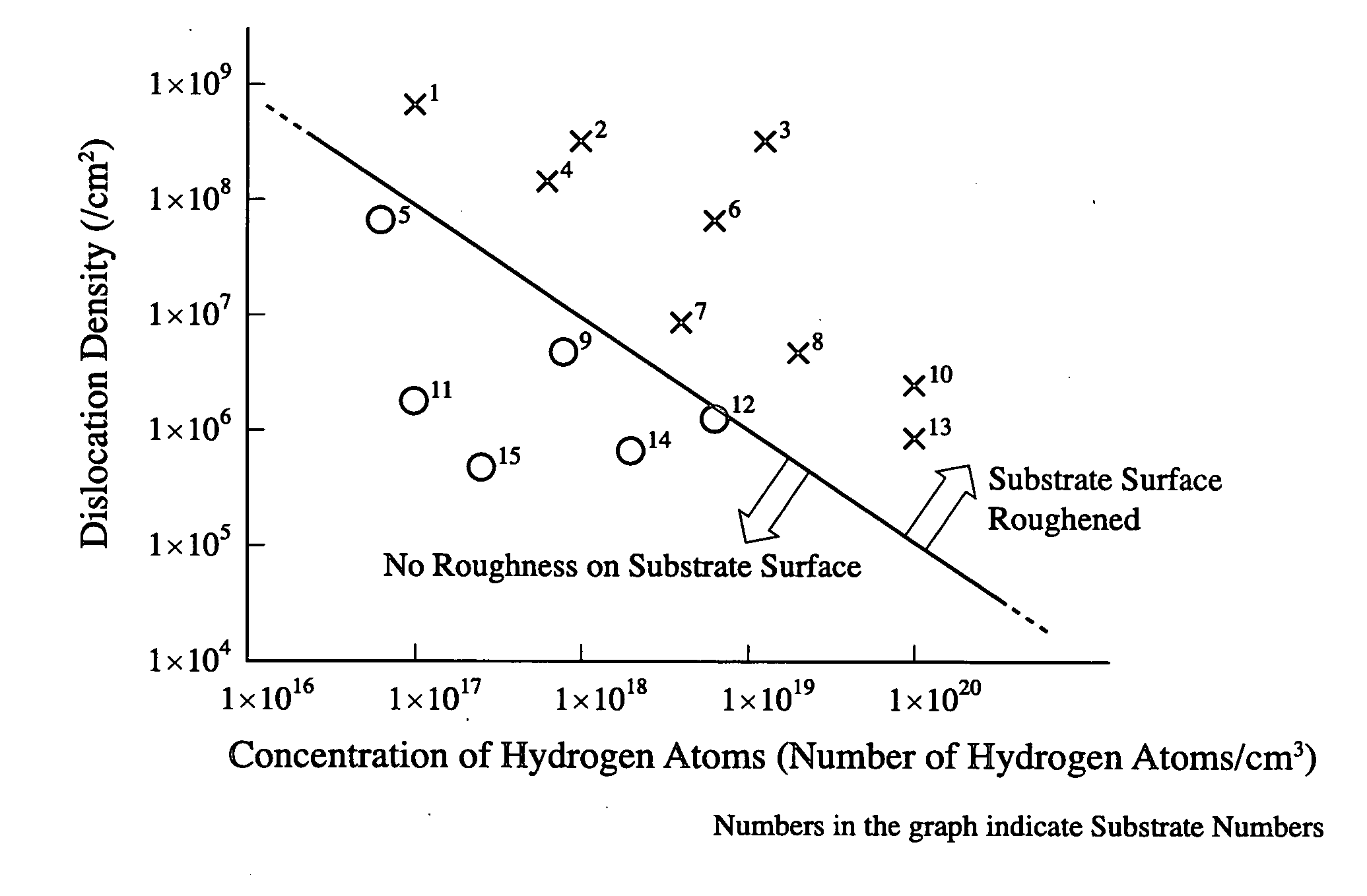
[0045] 15 types in total of GaN templates and self-supported GaN substrates having different dislocation densities and concentrations of hydrogen atoms were produced by an MOVPE method, an MBE method or an HVPE method under different conditions. The production conditions of each substrate are shown in Table 1. The surfaces of the self-supported GaN substrates grown by a VAS method were mirror-polished.
[0046] Each GaN template by MOVPE or MBE was produced by growing a GaN layer on a sapphire base substrate via a low-temperature-grown GaN buffer layer. There were two types of GaN substrates produced by HVPE; one was a GaN substrate produced by ELO (ELO substrate), and the other was a self-supported GaN substrate produced by VAS (VAS self-supported substrate).
[0047] The ELO substrate was produced by growing a GaN layer by an MOVPE method on a GaN template produced by an MOVPE method using trimethyl gallium (TMG) and NH3 as source gases, with a striped SiO2 mask disposed on the GaN te...
example 2
[0053] A surface of a 2-inch-diameter single-crystal sapphire base substrate, whose plane direction was C-plane offset by 0.2° toward an m-axis, was thermally cleaned at 1200° C. for 10 minutes in a hydrogen gas atmosphere. With the base substrate temperature lowered to 600° C., a 20-nm-thick, low-temperature GaN buffer layer was grown on the sapphire base substrate at an atmospheric pressure by an MOVPE method using trimethyl gallium (TMG) and NH3 as source gases. With the base substrate temperature elevated to 1050° C., the low-temperature GaN buffer layer was then microcrystallized by a thermal treatment at 1050° C. for 5 minutes. This thermal treatment can reduce the density of initial nuclei of a subsequently grown GaN crystal, resulting in a relatively decreased dislocation density. A GaN epitaxial layer was grown to a thickness of 4 μm, by continuously supplying the source gases onto the resultant substrate. During the above process, the crystal growth rate was about 4 μm / hou...
example 3
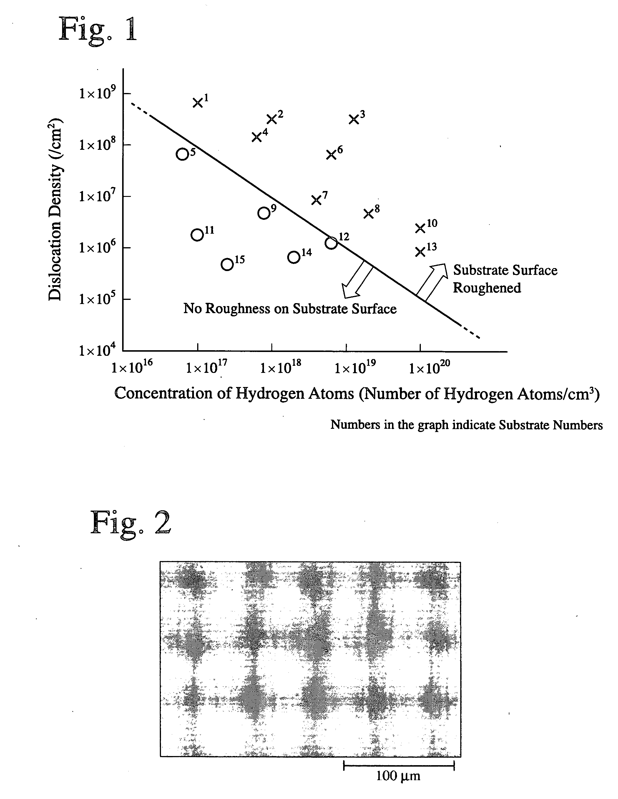
[0059] An undoped GaN layer was grown to a thickness of 300 nm on a C-plane of a 2-inch-diameter single-crystal sapphire base substrate using a low-temperature buffer technology by an MOVPE method using TMG and NH3 as source gases. A thin Ti film was vapor-deposited to a thickness of 20 nm on this undoped GaN layer. The resultant substrate was placed in an electric furnace, and thermally treated at 1050° C. for 20 minutes in an H2 stream containing 20% of NH3. As a result, part of the GaN layer was etched, resulting in voids at a high density (void layer), and the Ti layer was nitrided to have fine pores on the order of submicrons at a high density.
[0060] This substrate was placed in an HVPE chamber to grow a GaN layer to a thickness of 600 μm while supplying a gas containing source gases of GaCl at 8×10⁻³ atm and NH3 at 4.8×10⁻² atm in a carrier gas. The carrier gas was an N2 gas containing 5% of H2 in the first half of growth, and changed to an N2 gas only at a stage that the thi...
PUM
 Abstract
Description
Claims
Application Information