Stamper for producing optical recording medium, optical recording medium, and methods of producing the same

a technology of optical recording medium and stent, which is applied in the direction of flat record carrier container, record information storage, packaging, etc., can solve the problems of uneven thickness of inner and outer circumference, insufficient signal-to-noise ratio, and insufficient effect, so as to reduce the residual discrepancy of focus error, reduce the low frequency noise of disk signal, and improve the crosstalk characteristic

Inactive Publication Date: 2005-08-04
SONY CORP
View PDF12 Cites 11 Cited by
  • Summary
  • Abstract
  • Description
  • Claims
  • Application Information

AI Technical Summary

Benefits of technology

[0106] The above stamper may be used for injection molding to form a medium substrate having the relief shapes transferred to it. The stamper produced in the above way is suppressed in surface roughness, uneven thickness, deviation o...

Problems solved by technology

This appears as noise in a low frequency range and causes deterioration of the signal-to-noise (S/N) ratio.
As methods of smoothing the surface roughness and obtaining low signal noise, there are known the method of ashing by oxygen etc. after exposure and development as described in Japanese Examined Patent Publication (Kokoku) No. 7-29386 and the method of treatment by ultraviolet rays as described in Patent Gazette No. 2506983, however the effects thereof are not sufficient.
Further, the stamper used in the above method of production has to be produced to a thickness of at least 0.25 mm by high speed electroplating, so uneven thickness of the inner and outer circumferences occurs particularly easily.
In addition, since innumerable granular projections inevitably form on the plating film surface in the above electroplating, back polishing is essential, bu...

Method used


Image

  • Stamper for producing optical recording medium, optical recording medium, and methods of producing the same
  • Stamper for producing optical recording medium, optical recording medium, and methods of producing the same
  • Stamper for producing optical recording medium, optical recording medium, and methods of producing the same

Examples


first embodiment

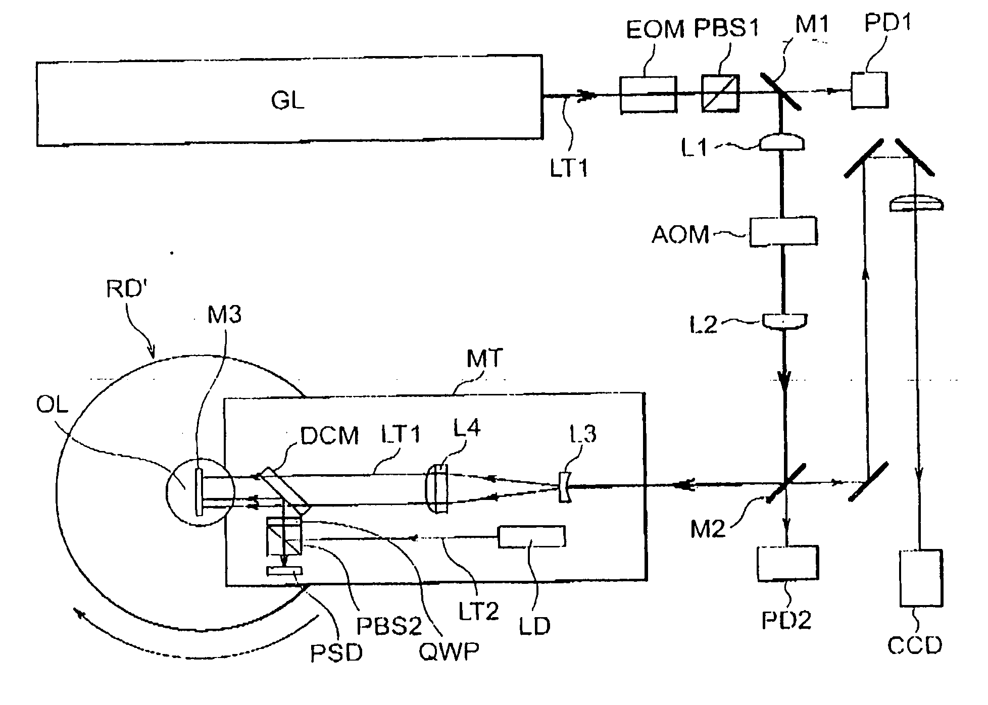
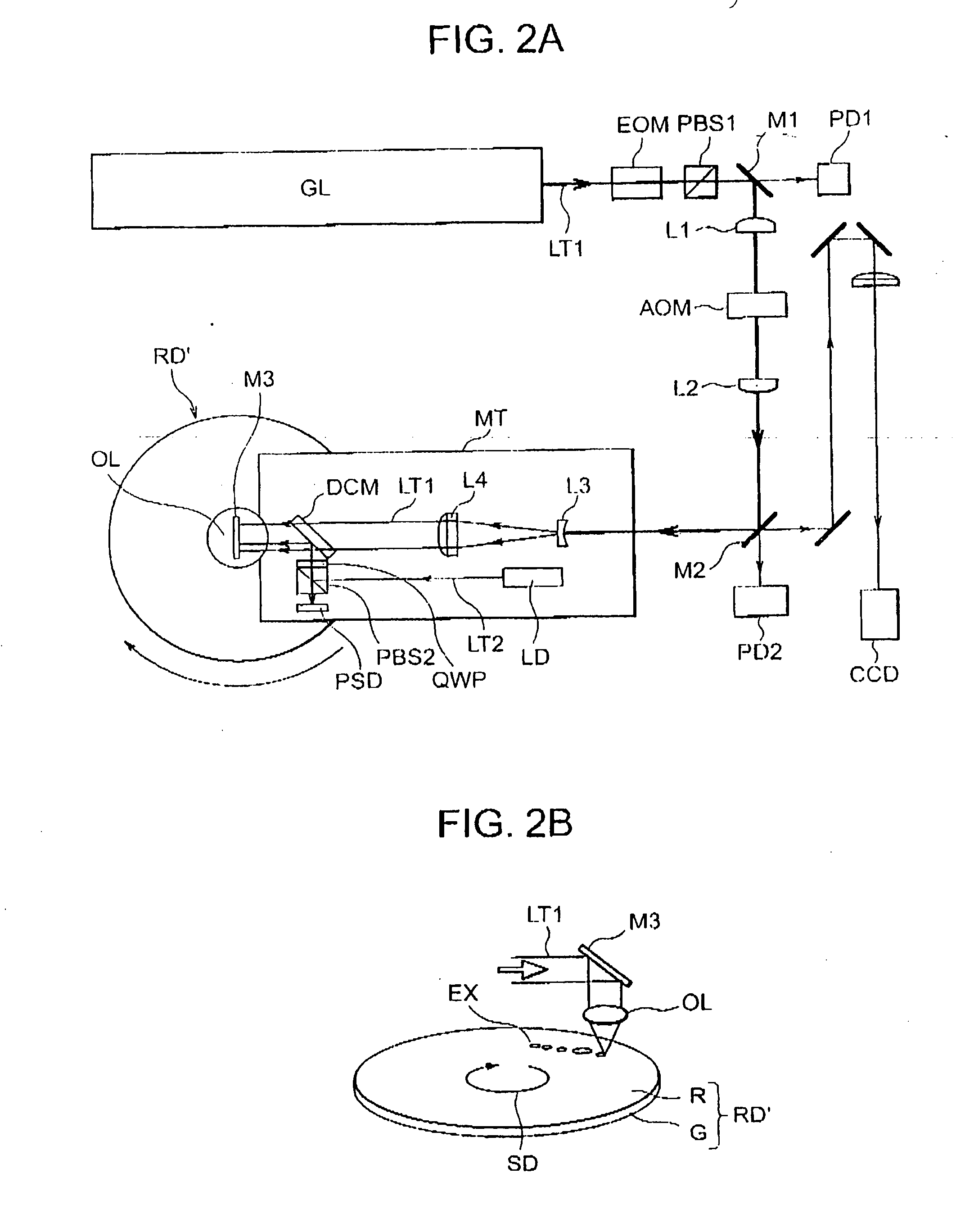
[0129]FIG. 7A is a schematic perspective view of a condition of irradiating an optical disk according to the present invention with light.

[0130] An optical disk DC is substantially shaped as a disk with a center hole CH formed at its center and is driven to rotate in a drive direction DR.

[0131] When recording or reproducing information, a laser light of a blue to bluish violet color region or other light LT is focused on an optical recording multilayer film in the optical disk DC by an object lens OL having a numerical aperture of for example 0.8 or more.

[0132]FIG. 7B is a schematic cross-sectional view, while FIG. 7C is an enlarged cross-sectional view of principal portions of the schematic cross-sectional view in FIG. 7B.

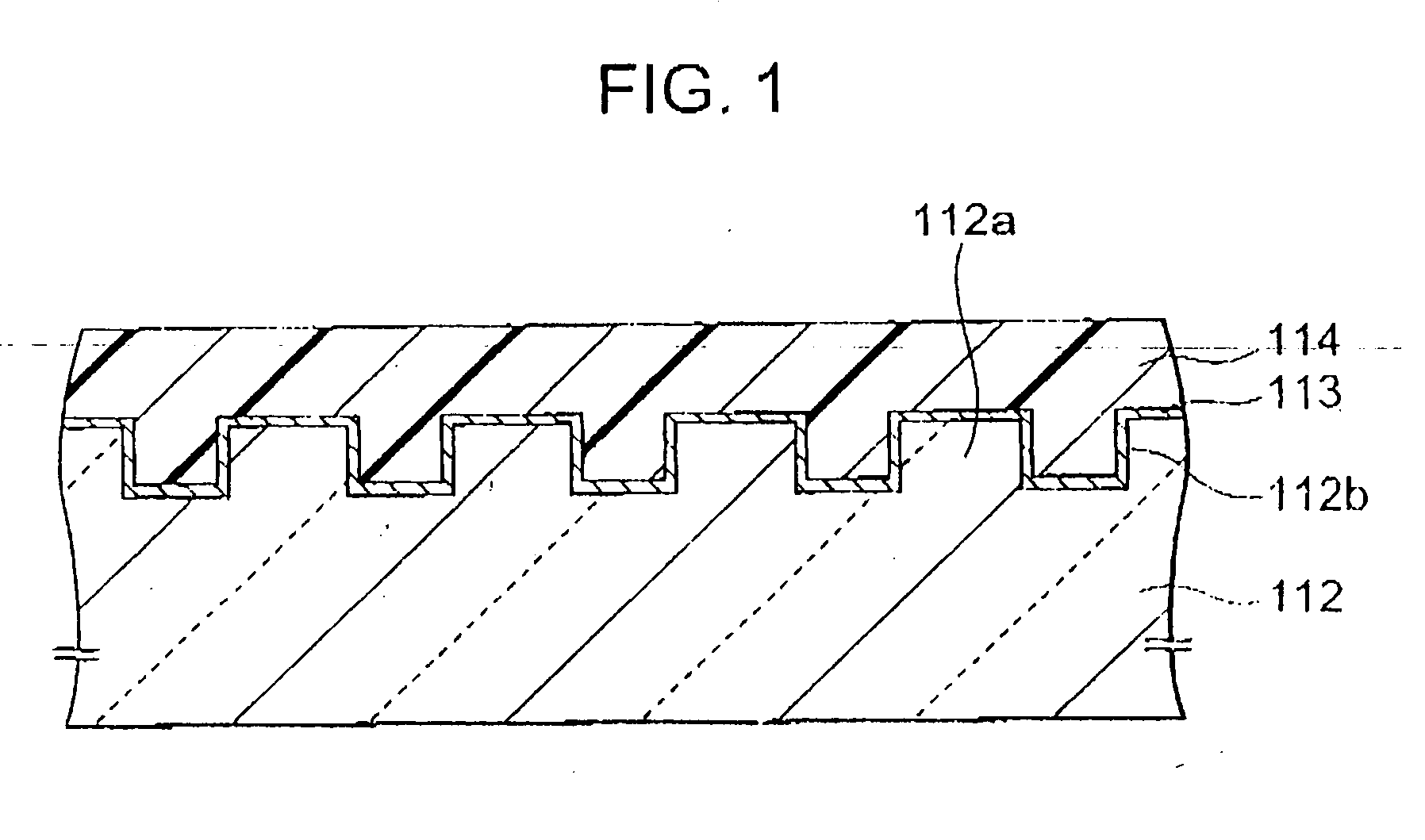
[0133] One surface of a disk substrate 12 having a thickness of about 1.1 mm and comprising polycarbonate, is provided with projecting regions 12a and recessed regions 12b defining track regions. That surface is further formed with an optical recording multila...

second embodiment

[0187]FIG. 12A is a schematic cross-sectional view of an optical disk of a second embodiment.

[0188] One surface of a disk substrate 20 having a thickness of about 1.1 mm and comprising polycarbonate is formed with projecting regions and recessed regions defining track regions. For example, a reflection film, a dielectric film, a recording film, another dielectric film, etc. are stacked in this order on this surface to form a first optical recording multilayer film 21. The configuration and number of layers of the first optical recording multilayer film 21 differ according to the type of the recording material and design. The above recording film includes for example a phase change type recording film, a magneto-optical recording film, and an organic pigment-containing recording film.

[0189] Further, over the first optical recording multilayer film 21 a second optical recording multilayer film 24 is formed via a light transmitting layer 22 comprising an ultraviolet curing resin etc....

third embodiment

[0215]FIG. 15A is a schematic cross-sectional view of an optical disk according to a third embodiment.

[0216] One surface of a disk substrate 34 having a thickness of about 1.1 mm comprising polycarbonate etc. is provided with projecting regions and recessed regions defining track regions. For example, a reflection film, a dielectric film, a recording film, another dielectric film, etc. are stacked in that order on this surface to form a first optical recording multilayer film 35. The configuration and number of layers of the first optical recording multilayer film 35 differ according to the type of recording material and design. The above recording film includes for example a phase change type recording film, a magneto-optical recording film, an organic pigment-containing recording film.

[0217] Further, over the first optical recording multilayer film 35 a second optical recording multilayer film 33 is formed via a light transmitting layer 36 comprising an ultraviolet curing resin ...


PUM

PropertyMeasurementUnit
Circumferenceaaaaaaaaaa

Abstract

A stamper suppressed in surface roughness, uneven thickness, and deviation of circularity in inner circumference, a method of producing the same, an optical recording medium produced by molding using the stamper, and a method of producing the same, wherein a base member having a mirror polished main surface and comprising silicon or glass is formed with a resist film; the resist film is exposed by a focused electron beam, an ultraviolet ray laser, etc. and developed so as to form a resist film of a pattern corresponding to relief shapes; the mirror surface of the base member is processed to relief shapes (projecting regions and recessed regions) by dry etching etc. using the obtained resist film as a mask so as to obtain a stamper; the obtained stamper is used for injection molding to form a medium substrate; and an optical recording multilayer film and a protective layer are formed to thereby produce an optical recording medium.

Description

BACKGROUND OF THE INVENTION [0001] 1. Field of the Invention [0002] The present invention relates to a stamper used in a process of producing an optical recording medium (hereinafter also referred to as an “optical disk”), an optical recording medium, and methods of producing the same. [0003] 2. Description of the Related Art [0004] In recent years, along with the advances made in technology for recording moving pictures, still images, and other video data in a digital format, compact disk (CD), digital versatile disk (DVD), and other optical disk apparatuses have been spotlighted as large capacity recording apparatuses. Research is underway for further increasing their capacity. [0005]FIG. 1 is a cross-sectional view of principal parts of an optical disk of the related art. [0006] One surface of a light transmitting disk substrate 112 made of for example polycarbonate is provided with projecting regions 112a and recessed regions 112b defining track regions. [0007] That surface has ...

Claims


Application Information

Patent Timeline
IPC IPC(8): G11B11/105B29C35/08B29C43/02B29C43/18B29C43/20B29C45/26B29D17/00G11B7/007G11B7/26G11B9/10
CPCB29C35/0888B29C43/021B29C43/18B29C43/203B29C45/2632G11B9/10B29C2043/025B29D17/005G11B7/00718G11B7/263B29C2035/0827G11B7/26
Inventor TAKEDA, MINORUARAKAWA, NOBUYUKIFURUKI, MOTOHIROIMANISHI, SHINGO
Owner SONY CORP
Why Eureka
Try Eureka