Silicon carbide single crystal and a method for its production

a single crystal, silicon carbide technology, applied in the direction of polycrystalline material growth, gel state, condensed vapor, etc., can solve the problems of stacking fault, fatal defects of micropipes, structural defects, etc., and achieve the effect of convenient handling

Inactive Publication Date: 2005-08-25
NIPPON STEEL CORP
View PDF4 Cites 43 Cited by
  • Summary
  • Abstract
  • Description
  • Claims
  • Application Information

AI Technical Summary

Benefits of technology

[0025] The term “bulk silicon carbide single crystal” used herein indicates a silicon carbide single crystal having a thickness of at least 50 micrometers. From the viewpoint of mechanical strength, the thickness of a bulk silicon carbide single crystal is preferably at least 200 micrometers, which makes it easy to handle a single crystal as a substrate material, and more preferably at least 500 micrometers, and most preferably at least 1500 micrometers.

Problems solved by technology

This leads to the occurrence of structural defects such as micropipes and stacking faults.
Stacking faults are caused by disorder or disturbance in stacking sequence of layers due to dislocation in crystal.
In particular, micropipes are fatal defects, and those portions of a single crystal including micropipe defects cannot be used for substrates.
Silicon carbide single crystals grown by the PVT technique include many structural defects such as micropipe defects and stacking faults.
The formation of many structural defects in the PVT technique is caused by the facts that it is quite difficult to control the partial pressures of these various vapors in a stoichiometric manner and that complicated reactions are involved in the crystal growth.
Nevertheless, bulk silicon carbide single crystals have mostly been produced by the PVT technique for the reason that it is extremely difficult for the other techniques to stably produce a bulk silicon carbide single crystal at a satisfactory growth rate, as described below.
Because bulk silicon carbide single crystals produced by the PVT technique include many micropipe defects, it is difficult to produce from these crystals semiconductor devices of a square shape measuring a few millimeters with a good yield.
The CVD technique is not suitable for the production of a bulk single crystal, which is required to manufacture a silicon carbide substrate, due to limited amounts of the raw materials being supplied in gaseous states.
It is not possible for the Acheson method to produce a pure silicon carbide single crystal due to contamination of the raw materials with many impurities, and it is also not possible for that method to obtain a single crystal having a size sufficient for use as a substrate material.
However, since the concentration of carbon dissolved from a graphite crucible into a melt is low, the growth rate of a silicon carbide crystal is very slow.
It is theoretically possible to increase the growth rate by elevating the temperature of the melt to 2000° C. or higher so as to increase the concentration of carbon which can be dissolved into the melt, but this results in severe evaporation of the Si solvent at atmospheric pressure, or if the melt is pressurized, the apparatus becomes complicated, either result being problematic for commercial production.
However, even if such a technique is employed, a product which has been actually obtained by the Si solvent method is merely a thin film having a thickness on the order of a few micrometers.
Accordingly, like the CVD technique, the solution growth technique has been considered to be a technique suitable for forming a thin film on a seed substrate but unsuitable for the growth of a bulk single crystal.
In that method, however, carbon is not supplied by dissolution from the graphite crucible.
Therefore, competitive dissolution of carbon from the crucible and from the raw material occurs inevitably.

Method used


Image

  • Silicon carbide single crystal and a method for its production
  • Silicon carbide single crystal and a method for its production
  • Silicon carbide single crystal and a method for its production

Examples


example 1

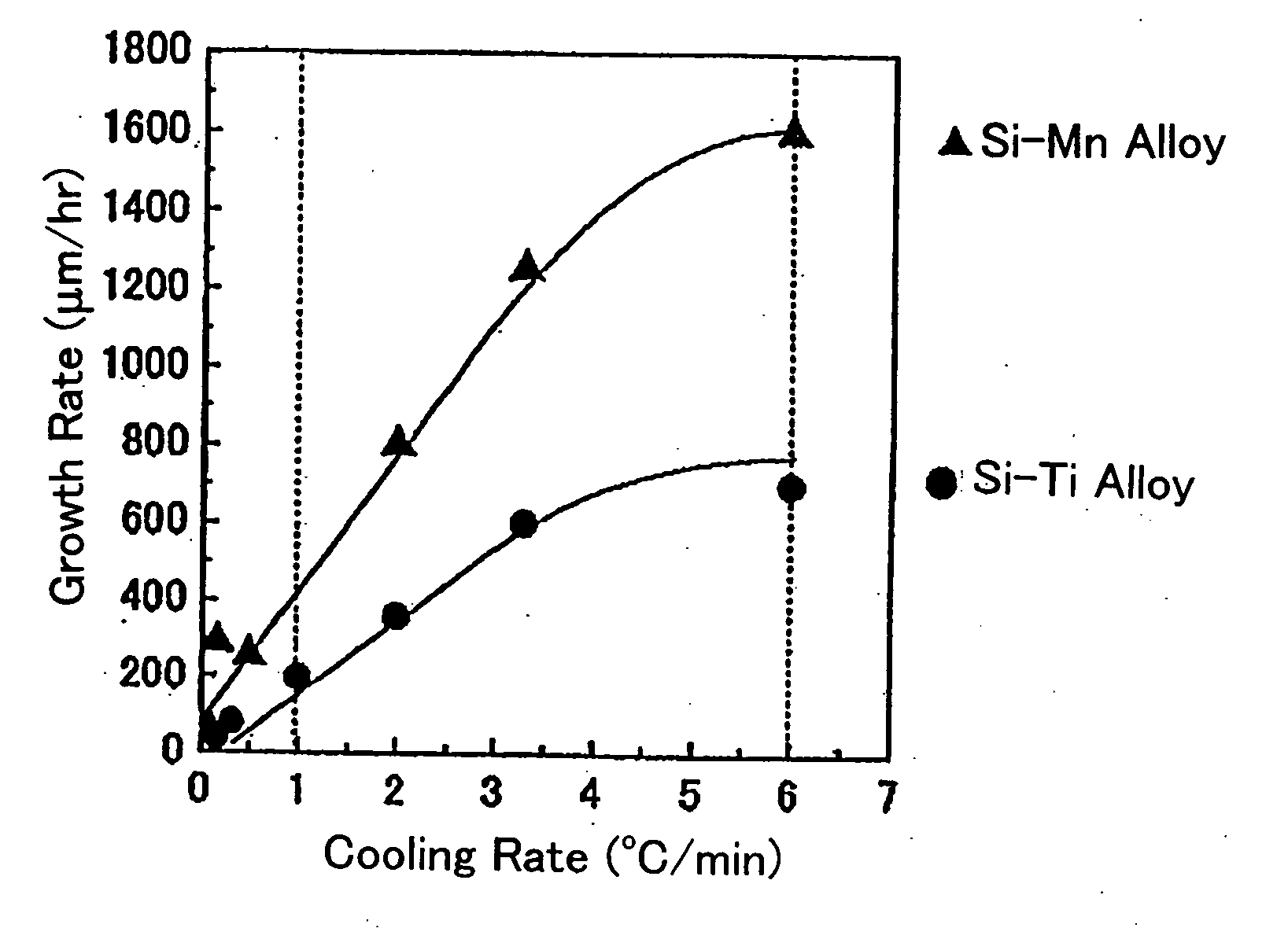
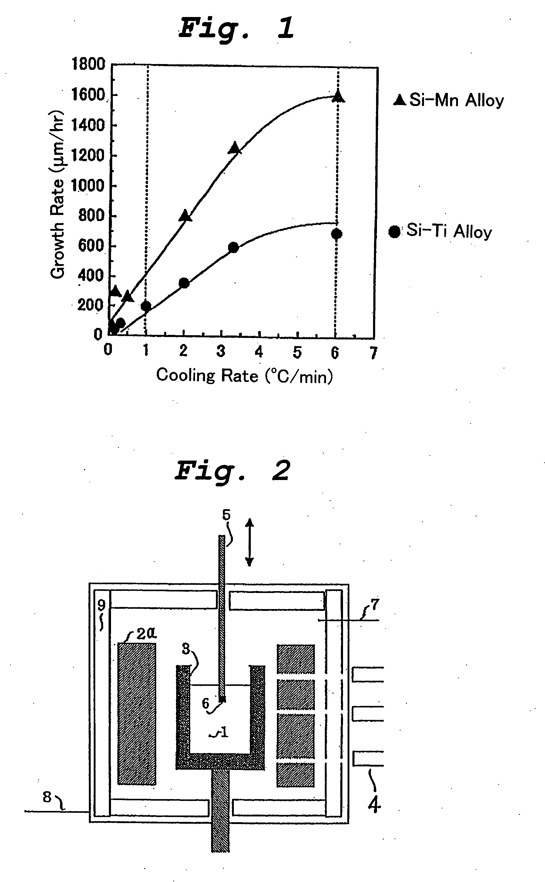
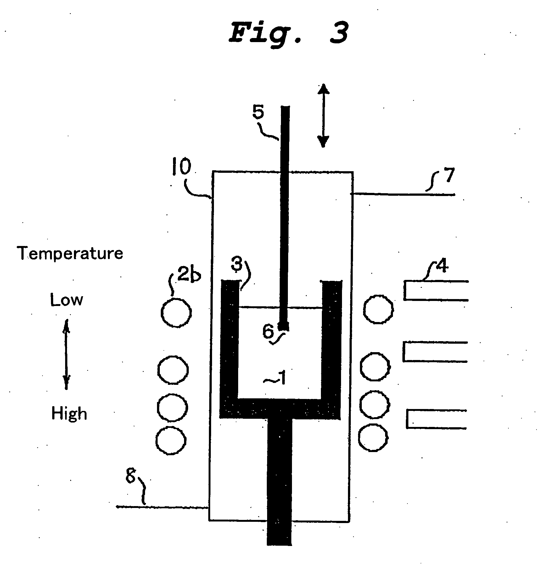
[0053] This example illustrates the production of a bulk silicon carbide single crystal by the cooling method using a crystal growth apparatus as shown in FIG. 2.

[0054] The crystal growth apparatus shown in FIG. 2 comprises a graphite crucible 3 containing an alloy melt 1, and the crucible 2 is encircled with a resistance heater 2a made of highly purified graphite. The resistance heater 2a and the graphite crucible 3 are enclosed within a thermal insulator 9. The temperature of the side wall of the graphite crucible 3 is directly measured by a plurality of optical pyrometers 4 through sight holes formed in the heater 2a and the thermal insulator 9. The heater 2a is controlled by the temperatures measured by these pyrometers 4 such that the crucible 3 is heated almost isothermally at a predetermined temperature. The atmosphere in the crystal growth apparatus is adjusted to an Ar atmosphere using a gas inlet 7 and a gas outlet 8.

[0055] The graphite crucible 3 was charged with raw ma...

example 2

[0061] A bulk silicon carbide single crystal was grown on a seed substrate 6 by the cooling method in the same manner as in Example 1 except that the graphite crucible 3 was charged with raw alloy materials having a composition of Si0.4Mn0.6 and heated at 1650° C. to melt the raw materials and that cooling was carried out from that temperature to 1450° C.

example 3

[0062] A bulk silicon carbide single crystal was grown on a seed substrate 6 by the cooling method in the same manner as in Example 2 except that the cooling rate was increased to 2° C. / min.


PUM

PropertyMeasurementUnit
temperatureaaaaaaaaaa

Abstract

A bulk silicon carbide single crystal of good crystalline quality which includes a minimized number of structural defects and is free from micropipe defects can be produced by crystal growth in a melt of an alloy comprising Si, C, and M (wherein M is either Mn or Ti) and having an atomic ratio between Si and M in which the value of x, when express as Si1-xMx, is 0.1≦×≦0.7 in the case where M is Mn or 0.1≦×≦0.25 in the case where M is Ti at a temperature of the melt which is below 2000° C. The C component is preferably supplied into the melt by dissolution of a graphite crucible which contains the melt such that the melt is free from undissolved C. One method of crystal growth is performed by cooling the melt after a seed substrate is immersed in the melt.

Description

TECHNICAL FIELD [0001] The present invention relates to a method for producing a bulk single crystal of silicon carbide (SiC) of good crystalline quality which is suitable for use as a substrate material for optical devices and electronic devices, and more particulary to a method capable of stably producing such a silicon carbide single crystal at a temperature of 2000° C. or lower, which is preferred from the viewpoint of operation. The present invention also relates to a bulk silicon carbide single crystal of good crystalline quality which is thus prepared. BACKGROUND ART [0002] Silicon carbide (SiC) is a class of thermally and chemically stable compound semiconductors and is characterized by having a band gap of about three times, a dielectric breakdown voltage of about ten times, a rate of electron saturation of about two times, and a coefficient of thermal conductivity of about 3 times as large as that of silicon (Si). In view of these favorable properties, silicon carbide is e...

Claims


Application Information

Patent Timeline
Patent Type & Authority Applications(United States)
IPC IPC(8): C30B11/00C30B29/36
CPCC30B29/36C30B11/00
Inventor KUSUNOKI, KAZUHIKOMUNETOH, SHINJIKAMEI, KAZUHITO
Owner NIPPON STEEL CORP
Why Eureka
Try Eureka