

Method for producing material of electronic device
- Summary
- Abstract
- Description
- Claims
- Application Information
AI Technical Summary
Benefits of technology
Problems solved by technology
Method used
Image

Examples
embodiment of
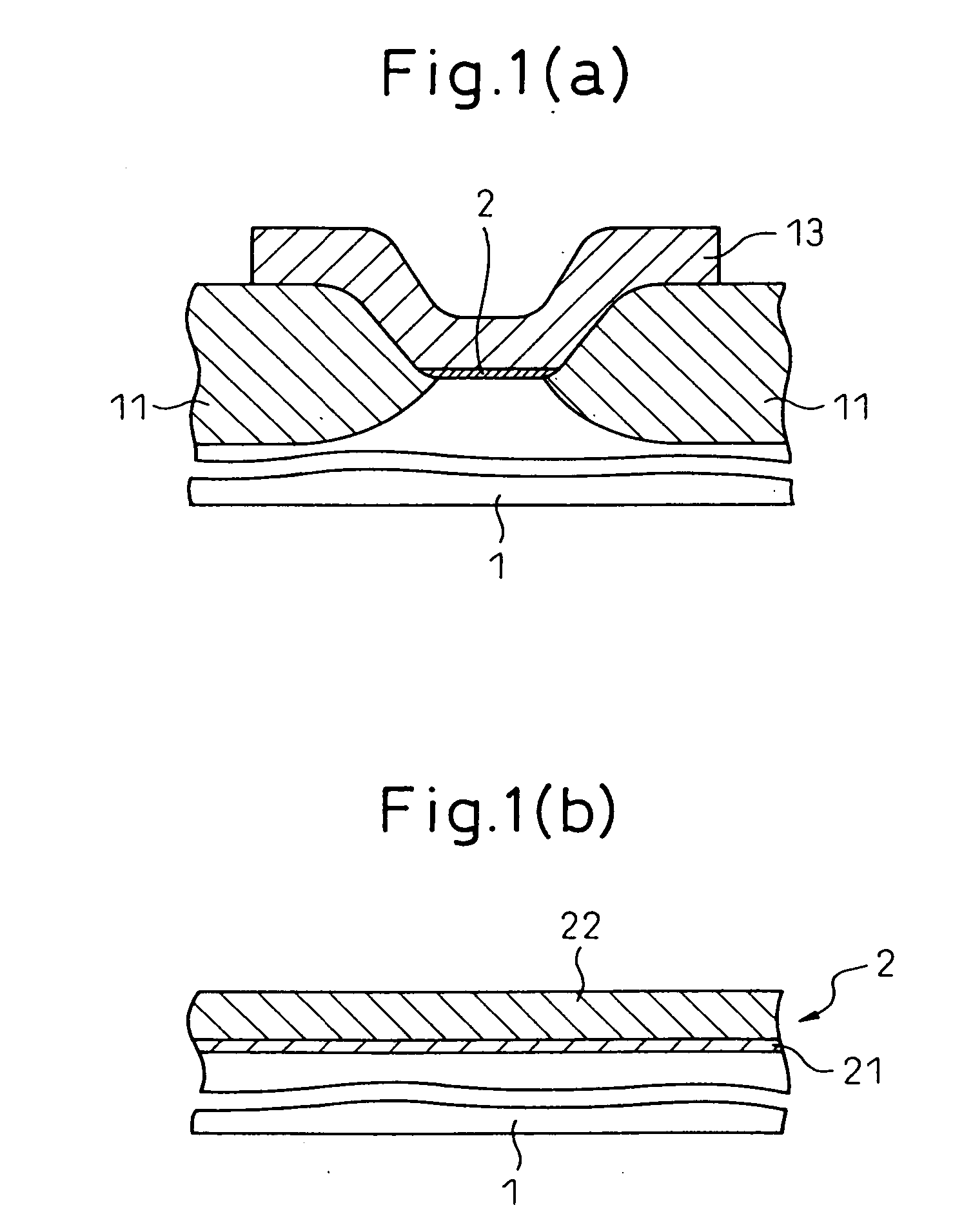
(One Embodiment of Production process)
[0072] Next, the process for producing such an electronic device material where a gate insulator 2 is provided and a gate electrode 13 is further provided thereon is described below.
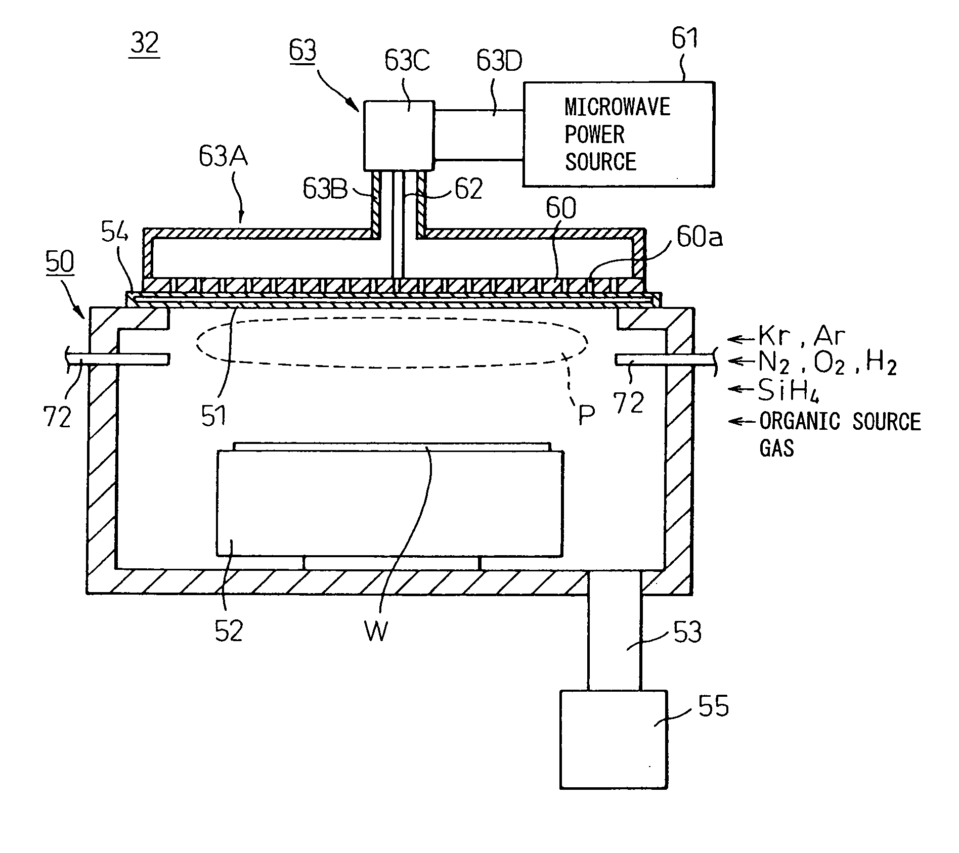
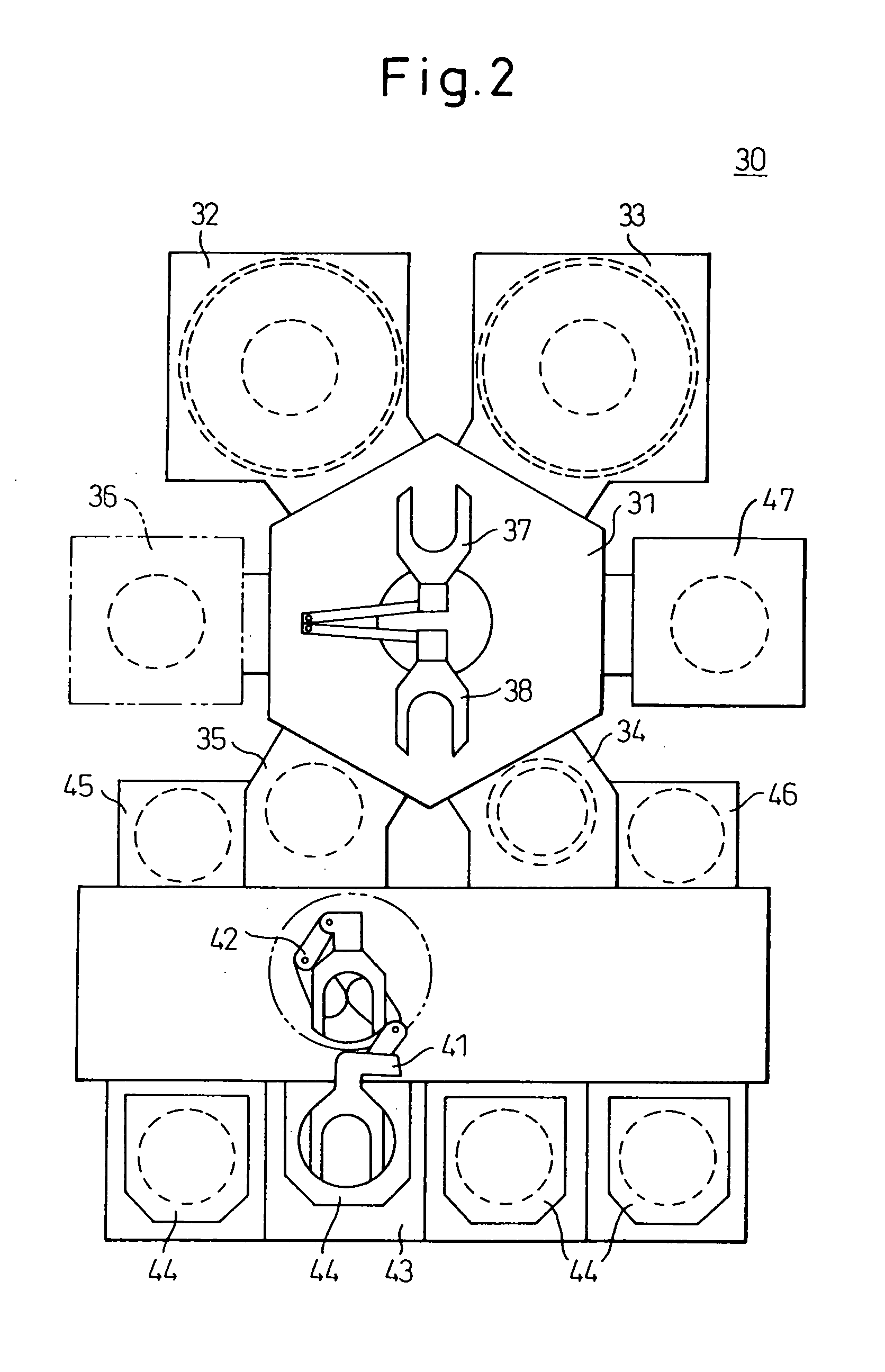
[0073]FIG. 2 is schematic view (schematic plan view) showing an example of the total arrangement of a semiconductor manufacturing equipment 30 for conducting the process for producing an electronic device material according to the present invention.
[0074] As shown in FIG. 2, in a substantially central portion of the semiconductor manufacturing equipment 30, there is disposed a transportation chamber 31 for transporting a wafer W (FIG. 3). Around the transportation chamber 31, there are disposed: plasma processing units 32 and 33 for conducting various treatments on the wafer, two load lock units 34 and 35 for conducting the communication / cutoff between the respective processing chambers, a heating unit 36 for operating various heating treatments, and a heating reac...
examples
[0125]FIG. 8 shows a profile by Auger electron spectroscopy of ZrO2 produced by the ordinary thermal CVD (M. A. Cameron and S. M. Geage, Thin Solid Films, 348 (1999), 90-98). The abscissa denotes the sputtering time (corresponding to the film thickness in the depth direction) and the ordinate denotes the content. As shown in the figure, it is understood that 10 to 20% of carbon content (C) is contained in the film.
[0126]FIG. 9 shows a carbon content in ZrO2 film which has been produced by using ECR plasma CVD (excerpt from Byeong-Ok Cho, Sandy Lao, Lin Sha and Jane P. Chang, Journal of Vacuum Science and Technology, A 19(6) (November / December 2001), pp. 2751-2761). The abscissa denotes the plasma emission intensity ratio and the ordinate denotes the carbon concentration in the film determined by the XPS analysis. The emission intensity ratio on the abscissa is described below. When plasma is subjected to an emission analysis by OES (optical emission spectroscopy), the light at a wa...
PUM
| Property | Measurement | Unit |
|---|---|---|
| Fraction | aaaaa | aaaaa |
| Energy | aaaaa | aaaaa |
| Concentration | aaaaa | aaaaa |
Abstract
Description
Claims
Application Information