
Laser irradiation apparatus

Active Publication Date: 2005-11-10
SEMICON ENERGY LAB CO LTD
View PDF50 Cites 30 Cited by
  • Summary
  • Abstract
  • Description
  • Claims
  • Application Information

AI Technical Summary

Benefits of technology

[0015] It is an object of the present invention to solve the above problems. Specifically, it is an object of the present invention to provide a laser irradiation apparatus capable of forming a laser beam having a shape required for annealing and having homogeneous energy distribution by providing a slit in which a slit opening (portion) has changeable length at an image-forming position of a diffractive optical element.
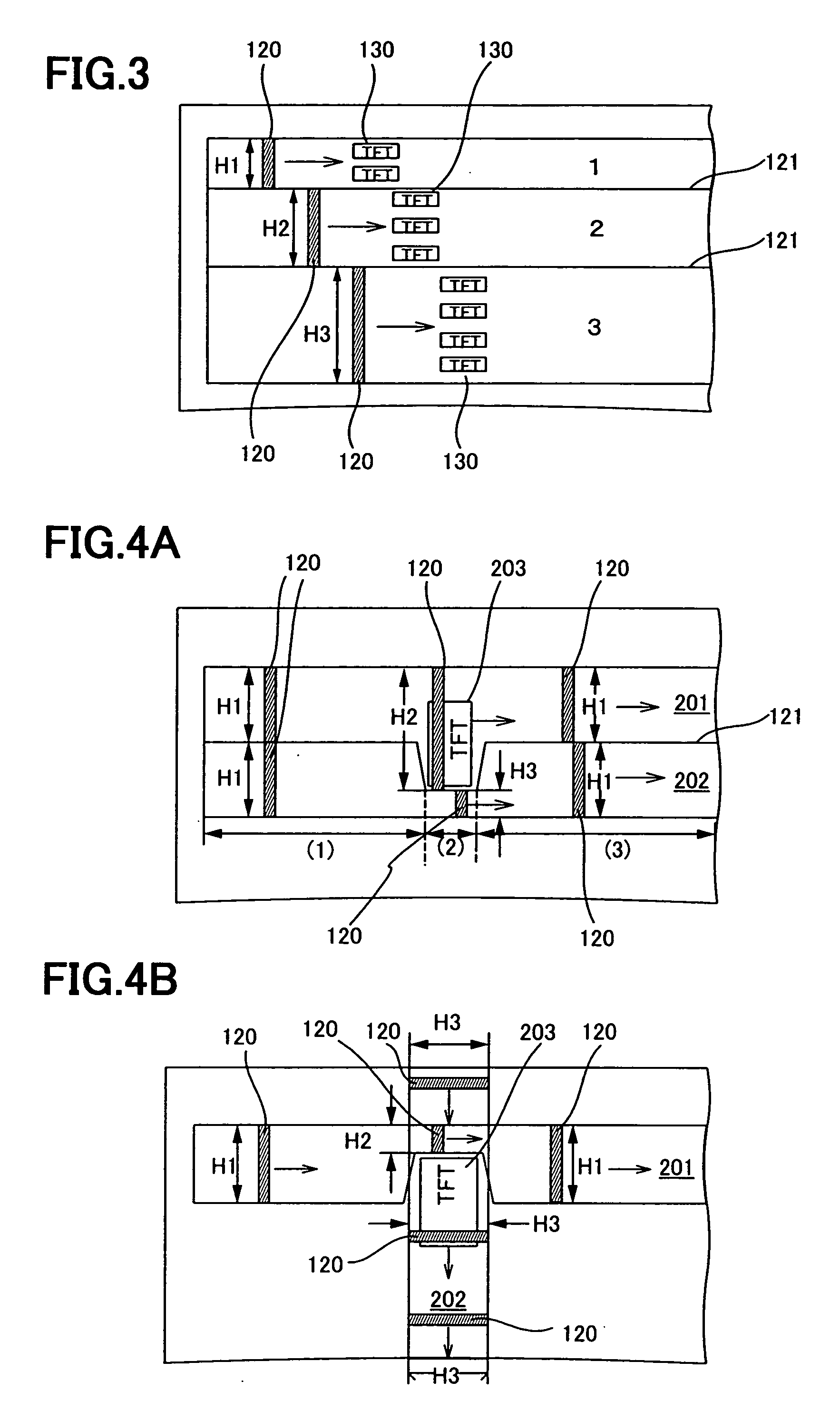
[0024] Further, when the length of the slit opening in the major-axis direction is changed in a direction perpendicular to the traveling direction of the laser beam, the end portions of the rectangular beam can be blocked and the laser beam can be shaped into a desired size. Accordingly, the optical alignment or the replacement of the optical component is no longer necessary, and rectangular beams of various sizes can be formed in short time.
[0025] Moreover, since the size of the rectangular beam can be changed easily in accordance with devices to be manufactured, many substrates can be processed in short time, which leads to the high throughput. Furthermore, since homogeneous annealing can be performed on the substrate, the homogeneity of the crystallinity within the substrate can be enhanced. For this reason, the variation in the electric characteristic can be decreased; therefore, the reliability can be enhanced. When the present invention is applied to a mass-production line for TFTs, it is possible to manufacture TFTs with high operating characteristic effectively.
[0026] As a result, the operating characteristic and the reliability of the semiconductor device, typically an active matrix type liquid crystal display device, can be enhanced. Moreover, the manufacturing process of the semiconductor device can have a wider margin to boost the yield; therefore, the manufacturing cost of the semiconductor device can be decreased.

Problems solved by technology

However, the laser annealing with a continuous wave laser oscillator has a problem in that an annealed state of an irradiation surface becomes inhomogeneous.
Accordingly, homogeneous annealing is difficult to achieve.
However, since the conventional laser irradiation apparatus needs to use a plurality of expensive cylindrical lens arrays and to arrange them so as to form a desired linear beam as described above, the apparatus has a problem in that the size and cost of the apparatus increases.
Therefore, optical alignment is required every time the size of the linear beam is changed, which consumes a large amount of time.
This results in the low throughput (see Reference 1: Japanese Patent Application Laid-Open No: 2003-257885).
However, the above laser irradiation apparatus still has a problem of inhomogeneous energy distribution at the end portions of the rectangular beam.
Moreover, since it is necessary to replace the diffractive optical element or other lenses or to rearrange the optical elements in order to change the size of the beam, the optical alignment takes much time, thereby resulting in the low throughput.

Method used


Image

  • Laser irradiation apparatus
  • Laser irradiation apparatus
  • Laser irradiation apparatus

Examples


embodiment 1

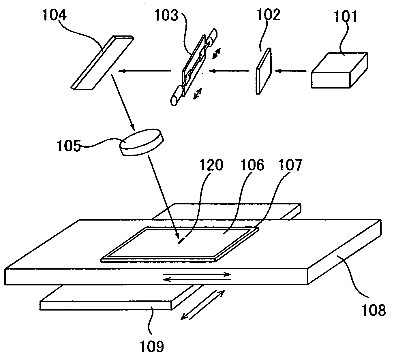
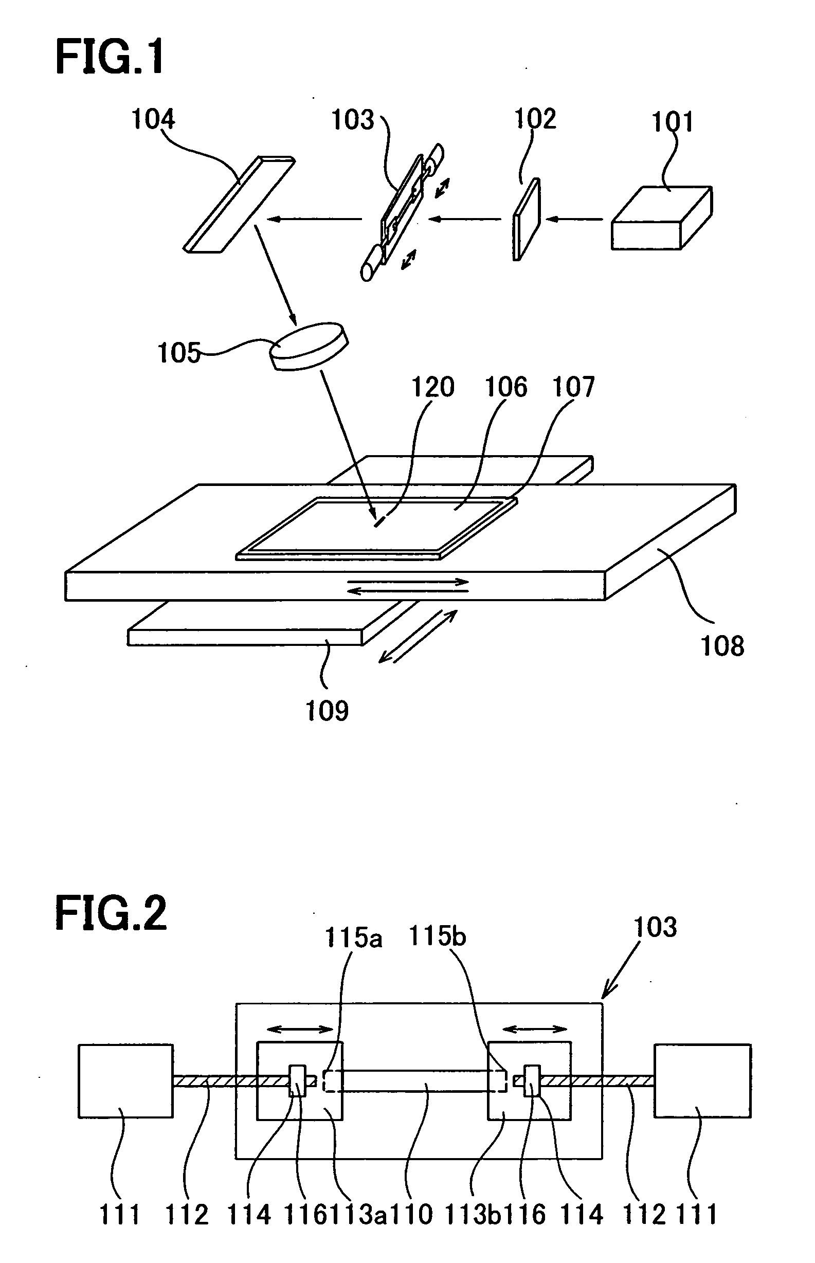
[0038]FIG. 1 shows an example of a laser irradiation apparatus according to the present invention. First, a substrate 107 with a non-single crystal semiconductor film 106 formed is prepared. The substrate 107 is mounted over an X-axis stage 108 and a Y-axis stage 109. The substrate 107 can be moved freely in an X-axis direction and a Y-axis direction by moving the X-axis stage 108 and the Y-axis stage 109 with a motor (not shown) respectively in directions indicated by arrows in FIG. 1.

[0039] The laser irradiation apparatus comprises a laser oscillator 101, a diffractive optical element 102, a slit 103, a mirror 104, and a condensing lens 105. As the condensing lens 105, a convex lens (a spherical lens or a convex cylindrical lens) can be used. As the laser oscillator 101, a known continuous wave laser or a solid-state laser can be used. The continuous wave laser is a laser having a single crystal or a poly crystal as a medium. YAG, YVO4, YLF, YAlO3, GdVO4, alexandrite, or Ti:sapph...

embodiment 2

[0056] This embodiment shows a process for forming a thin film transistor (TFT) with a laser annealing apparatus according to the present invention.

[0057] Initially, a base film 801 is formed over a substrate 800 as shown in FIG. 8A. A glass substrate made from, for example, barium borosilicate glass or alumino borosilicate glass, a quartz substrate, a ceramic substrate, or a stainless substrate can be used as the substrate 800. In addition, although a substrate made from flexible material such as acrylic or plastic tends to be inferior to the above substrates in point of heat resistance, the substrate made from flexible material can be used when the substrate can resist the processing temperature of the following manufacturing steps.

[0058] The base film 801 is provided in order to prevent the alkali-earth metal or alkali metal such as Na included in the substrate 800 from diffusing into the semiconductor film. The alkali-earth metal or alkali metal causes an adverse effect on the...

embodiment 3

[0076] According to the present invention, various electronic apparatuses can be completed with thin film transistors. FIGS. 10A to 10C illustrate the specific examples.

[0077]FIG. 10A shows a display device including a chassis 1001, a supporting stand 1002, a display portion 1003, speaker portions 1004, video input terminals 1005, and the like. This display device is manufactured using the thin film transistor manufactured by Embodiment 1 or 2 in the display portion 1003. The display device includes a liquid crystal display device, a light-emitting device, and the like. Specifically, the display device includes all kinds of display device for displaying information such as a display device for a computer, television reception, and advertisement.

[0078]FIG. 10B shows a computer including a chassis 1011, a display portion 1012, a keyboard 1013, an external connection port 1014, a pointing mouse 1015, and the like. By using the manufacturing method shown in Embodiment 1 or 2, the pres...


PUM

PropertyMeasurementUnit
Frequencyaaaaaaaaaa
Lengthaaaaaaaaaa
Distributionaaaaaaaaaa

Abstract

The present invention is to provide a laser irradiation apparatus for forming a laser beam which has a shape required for the annealing and which has homogeneous energy distribution, by providing a slit at an image-formation position of a diffractive optical element, wherein the slit has a slit opening whose length is changeable. The laser irradiation apparatus comprises a laser oscillator, a diffractive optical element, and a slit, wherein the slit has a slit opening whose length in a major-axis direction thereof is changeable, wherein a laser beam is delivered obliquely to a substrate, and wherein the laser beam is a continuous wave solid-state, gas, or metal laser, or a pulsed laser with a repetition frequency of 10 MHz or more.

Description

BACKGROUND OF THE INVENTION [0001] 1. Field of the Invention [0002] The present invention relates to a laser irradiation apparatus (an apparatus including a laser and an optical system for guiding a laser beam emitted from the laser to an irradiation object) for carrying out annealing to, for example, a semiconductor material homogeneously and effectively. [0003] 2. Related Art [0004] In recent years, a technique for manufacturing a thin film transistor (hereinafter referred to as a TFT) over a substrate has been developed drastically, and application to an active matrix display device has been advanced. In particular, a TFT formed using a poly-crystalline semiconductor film is superior in field-effect mobility to a TFT formed using a conventional amorphous semiconductor film, and therefore high-speed operation becomes possible when the TFT is formed using the poly-crystalline semiconductor film. For this reason, it has been tried that a driver circuit, which has been conventionally...

Claims


Application Information

Patent Timeline
IPC IPC(8): B23K26/00B23K26/06B23K26/073B23K26/08B23K26/40
CPCB23K26/063B23K26/0656B23K26/0732B23K26/0853B23K2201/40C30B29/52C30B11/005C30B11/04C30B13/22C30B28/08C30B29/06C30B1/023B23K2101/40B23K26/0622B23K26/066
Inventor TANAKA, KOICHIRO
Owner SEMICON ENERGY LAB CO LTD
Learn More