Build-up structures with multi-angle vias for chip to chip interconnects and optical bussing

a technology of optical bussing and build-up structures, which is applied in the direction of television systems, instruments, and semiconductor/solid-state device details, etc., can solve the problems of complex build-up on die processing, difficult work of providing escape routing through circuitry on the chip scale package, and even more problems, so as to improve the testability of the die, improve signal routing, and reduce the amount of required circuitry layers

Inactive Publication Date: 2005-12-08
CAPITALSOURCE FINANCE
View PDF10 Cites 51 Cited by
  • Summary
  • Abstract
  • Description
  • Claims
  • Application Information

AI Technical Summary

Benefits of technology

[0017] An object of the present invention is to develop a means by which entire electronic systems, preferably with multiple active and passive components, can be packaged into one multilayer structure thereby achieving improved performance at high speeds including excellent electrical, mechanical, thermal, cost, and reliability characteristics.
[0019] Another object of the present invention is the creation multi-angled electrical conductive and / or optical vias for improved signal routing between the chips, improved testability of the die during the process, reduction in the amount of required circuitry layers, and improvement in the reduction of stress of the integrated structure during thermal excursions and during operation of the system.
[0020] Another object of the present invention is to integrate advanced materials to achieve the electrical, mechanical, optical, and thermal properties required of this new structure including nanocomposites, mesocomposites, mesoporous materials, very high Tg (glass transition temperature) organic dielectrics, anisotropic conductive films, copper-invar-copper and other CTE controlled materials which provide low dielectric constants for high speed signal transmission and optical transmission while reducing stress in the finished system. Mesocomposites and mesoporous materials allow optical lasing, detection and wave guiding in addition to allowing formation of optical waveguides with either photo defined, laser, or soft-lithography methods. Also mesocomposites and mesoporous materials have extremely low dielectric constants, typically on the order of approximately 2.0K, which allows very fast signal transmission speeds in adjacent conductors while maintaining coefficient of thermal expansions in the same order of magnitude of semiconductor substrates (approximately 4-10 ppm / degree Centigrade). Very high Tg organic dielectrics (300 degrees Celsius) provide excellent toughness, elongation properties, and low CTE below the glass transition temperature of the material which provides an excellent dielectric material for build-up on die. Furthermore, certain polymers have excellent moisture barrier and moisture uptake properties such as Liquid Crystal Polymers (LCPs) that have excellent properties for integrating and protecting Microelectromechanical Machines (MEMs) components in the build-up process and in the final product.

Problems solved by technology

The work of providing escape routing through circuitry on the Chip Scale package becomes difficult as geometries keep shrinking.
Complex build-up on die processing suffers from technological constraints due to reliability and quality issues when temperature excursions (as in soldering) cause fractures in the composite which are due to Coefficient of Thermal Expansion (CTE) differences between the various materials and components of the package.
These issues are even more problematic when attempts are made to package multiple die of different geometries and materials in a monolithic structure.
For example, encapsulation materials of the embedded die and the design of the vias often result in an undesirably rigid structure which, combined with the CTE mismatch materials, causes delamination (adhesion failure) during a thermal stress or soldering operation.
Furthermore, the embedding of various components, such as sensors, MEMs (Micro Electromechnaical Machines), capacitors, resistors, inductors, transducers and antennas, each of which typically has a unique CTE, cannot be performed in multicomponent structures due to additional stress issues of the various materials and their different CTE values.
Another shortcoming of existing art is that it does not accommodate various component thicknesses during a multilayer structure embedding process because the build-up process requires a very level surface for the first dielectric and metal layers to be successful.
Each of these die substrate materials would have with their respective thickness profiles and the thickness difference's would not be suitable for existing build-up on die processes.
Still another shortcoming of build-up on die prior art is that it does not facilitate die electrical testing prior to embedding.
Semiconductor wafer processing techniques are known to have defects that are undetectable unless tested, and testing often occurs after the die is packaged.
In a build-up on die process, if a die is defective, the entire monolithic structure will be wasted because testing cannot be performed very early in the process.
Build-up on Die and Chip Scale packaging do not accommodate optical transmission of data between chips in either discrete component technologies or in monolithic technologies.
Existing build-up on die techniques do not accommodate the direct connection of optical components for die-to-die or component-to-component optical interconnections to tap into these higher bandwidths.
Build-up on die and Chip Scale packaging also have difficulty addressing thermal dissipation requirements of monolithic structures.
However, as performance increases, the die dissipate more heat energy during operation, and consequently a means of dissipating the heat to an external cooling source either passively by conduction or with an active system becomes more critical.
Existing build-up on die and CSP technologies have difficulty in removing excess heat during operation of the system.
Although commonly used, sharp, 90 degree structures have several disadvantages when utilized unilaterally throughout a structure in high speed, high density designs.
Both electrical signals and optical signals experience significant signal loss at a 90 degree bend.
Electrical signals radiate significant amounts of energy and noise at the 90 degree bend thereby degrading the signal.
Optical signals experience a more difficult hurdle because a relatively large percentage of the incoming optical light is reflected back to the source, never making the bend.
As the mismatch between the pitch of the die and the component increases, the likelihood of requiring more circuitry layers increases with 90 degree vias, thereby increasing the cost of the system.
In addition, 90 degree vias exhibit high degrees of stress between the via and the copper circuitry during a thermal excursion due to the CTE mismatch of copper circuitry and the dielectric materials.
Cracks often initiate at the interface between the via and copper circuitry which can result in a circuitry failure and an electrical open circuit.

Method used


Image

  • Build-up structures with multi-angle vias for chip to chip interconnects and optical bussing
  • Build-up structures with multi-angle vias for chip to chip interconnects and optical bussing
  • Build-up structures with multi-angle vias for chip to chip interconnects and optical bussing

Examples


Embodiment Construction

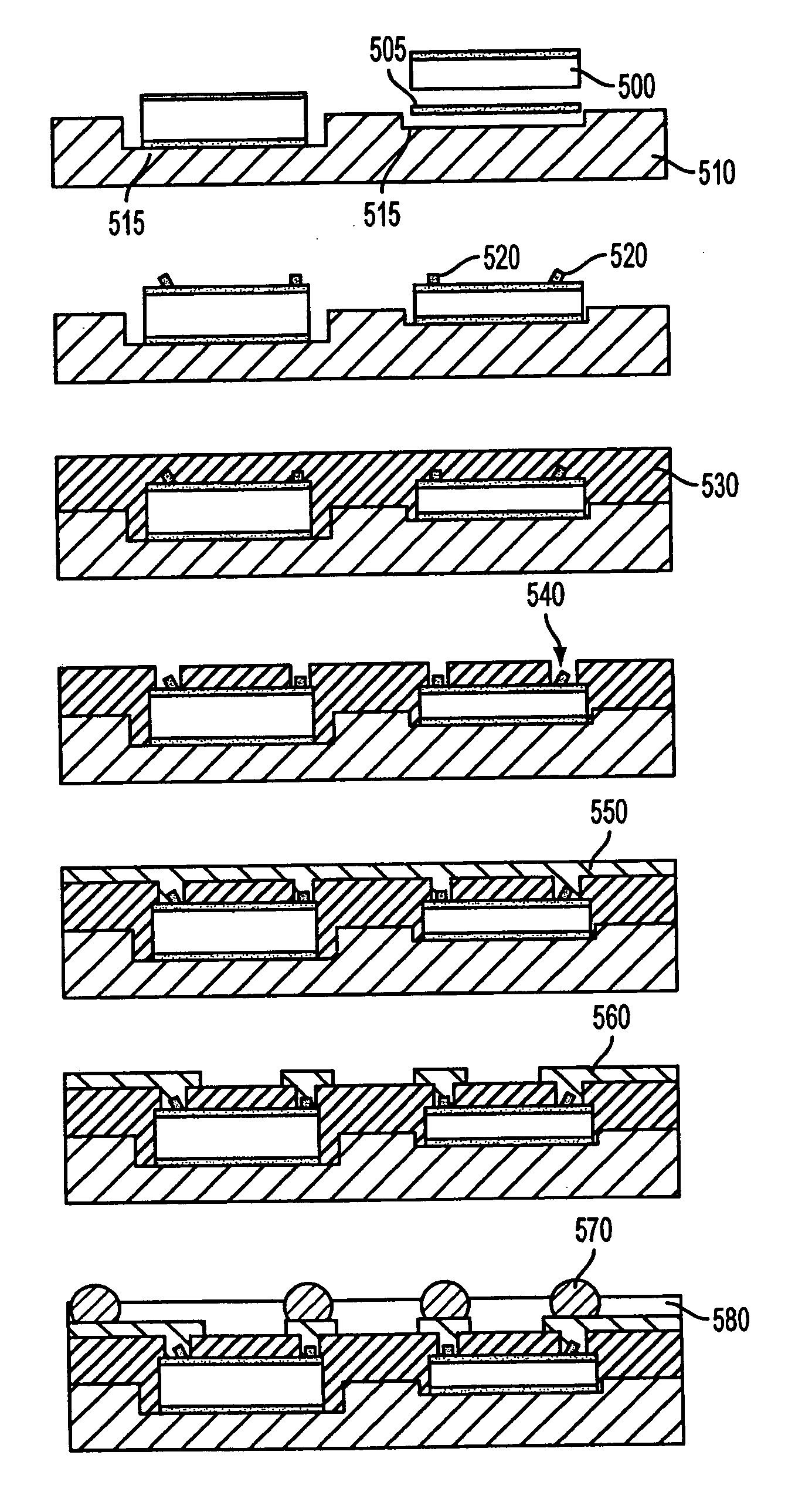
[0039] Reference will now be made in detail to preferred embodiments of the present invention, examples of which are illustrated in the accompanying drawings.

[0040] A build-up electrical structure that is fabricated with a build-up process and multi-angle vias for interconnecting die or multiple die and / or passive components such as capacitors, Microelectromechanical Machines (MEMs), Nanoelectromechanical Machines (MEMs), Bioelectromechanical Machines (BioMEMs), sensors, planar capacitors, resistors, planar resistors, inductors, fuel cells, antennas, thin film batteries, VCSEL's, photodiodes, or other active and passive components is described herein. Typical preferred process times and temperatures are 350° C. for one hour with normal prepregs, 250° C. for 90 seconds with mesoporous materials and 350° C. for 20 seconds for anistropic conductive adhesives. Typical process temperatures for very high Tg photo-imageable dielectrics would be 375° C. for 1 hour. Via formations are prefe...


PUM


Abstract

A build-up structure for chip to chip interconnects and System-In-Package utilizing multi-angle vias for electrical and optical routing or bussing of electronic information and controlled CTE dielectrics including mesocomposites to achieve optimum electrical and optical performance of monolithic structures. Die, multiple die, Microelectromechanical Machines (MEMs) and / or other active or passive components such as transducers or capacitors can be accurately positioned on a substrate such as a copper heatsink and multi-angle stud bumps can be placed on the active sites of the components. A first dielectric layer is preferably placed on the components, thereby embedding the components in the structure. Through various processes of photolithography, laser machining, soft lithography or anisotropic conductive film bonding, escape routing and circuitry is formed on the first metal layer. Additional dielectric layers and metal circuitry are formed utilizing multi-angle vias to form escape routing from tight pitch bond pads on the die to other active and passive components. Multi-angle vias can carry electrical or optical information in the form of digital or analog electromagnetic current, or in the form of visible or non-visible optical bussing and interconnections.

Description

PRIORITY CLAIM [0001] The present invention is related to, and claims priority from, Provisional U.S. Patent Application Ser. No. 60 / 424,710, the teachings of which are incorporated herein by reference in their entirety.FIELD OF THE INVENTION [0002] The present invention relates to the field of high density and high speed semiconductor packages and optical interconnects. In particular, the present invention provides build-up structures for interconnecting single or multiple semiconductor chips, Microelectromechanical Machines (MEMs) and / or die thereof of various thicknesses embedded in multilayer structures, a System-In-Package, Wafer-Scale Packages, or metal clad laminates utilizing multi-angle optical and / or electrical vias and controlled CTE dielectrics such as mesocomposites, to achieve electrical and optical performance. BACKGROUND OF THE INVENTION [0003] In the manufacturing of chip packaging, attempts have been made to maintain efficient interconnection between the die and ot...

Claims


Application Information

Patent Timeline
Patent Type & Authority Applications(United States)
IPC IPC(8): B81B7/00B81B7/02G02B6/43H01L21/60H01L23/31H01L23/433H01L23/538H05K1/02H05K1/11H05K1/18
CPCB81C1/0023H01L2224/73267H01L23/3128H01L23/4334H01L23/5389H01L24/24H01L24/27H01L24/82H01L24/83H01L2224/16225H01L2224/24227H01L2224/73204H01L2224/83101H01L2224/83191H01L2224/838H01L2224/92H01L2224/92244H01L2924/01005H01L2924/01013H01L2924/01029H01L2924/01032H01L2924/01078H01L2924/01079H01L2924/01082H01L2924/0781H01L2924/10329H01L2924/15153H01L2924/15165H01L2924/15311H01L2924/19041H01L2924/19042H01L2924/19043H01L2924/30107H05K1/0274H05K1/115H05K1/185H05K1/186H05K2201/09836H05K2203/061G02B6/43H01L2224/32245H01L2224/12105H01L2924/07811H01L24/29H01L2224/2919H01L2224/32225H01L2924/01006H01L2924/01019H01L2924/01033H01L2924/014H01L2924/0665H01L2924/0132H01L2224/83H01L2224/82H01L2924/00H01L2924/01014H01L2924/01031H01L2924/3512H01L2223/6677H01L2224/02333H01L2924/12042H01L2924/12043H01L2924/351
Inventor FORCIER, ROBERT
Owner CAPITALSOURCE FINANCE
Why Eureka
Try Eureka