Laser-ultrasonic detection of flip chip attachment defects

a flip chip and ultrasonic technology, applied in the field of electronic assemblies, can solve the problems of premature failure, limited device switching speed, and inability to provide the needed number of input/output connections, etc., and achieve the effect of avoiding ablation damage to the flip chip, enhancing the directivity and intensity of acoustic waves, and maximizing the acoustic bandwidth

Inactive Publication Date: 2006-02-02
OPTECH VENTURES +1
View PDF3 Cites 24 Cited by
  • Summary
  • Abstract
  • Description
  • Claims
  • Application Information

AI Technical Summary

Benefits of technology

[0010] The present invention provides a laser-ultrasonic method and device that are useful for detection of defects in the underfill and solder ball attachments between a flip chip and a substrate. In the method of the invention, a probe acoustic wave is generated in the flip chip by directing a generation laser beam of small diameter to a predetermined generation spot on the top surface of the flip chip. The acoustic bandwidth may be maximized by using a generation laser of a wavelength that is strongly absorbed by the flip chip semiconductor so that the laser light is absorbed in a thin region near the top surface of the flip chip. Alternatively, the wavelength of the generation laser light may be selected so as to distribute the light absorption over a greater volu...

Problems solved by technology

As electronics miniaturization progressed, chips become so small and densely packed with circuitry and circuit elements that even fine-pitched peripheral contacts could no longer provide the needed number of input/output (I/O) connections.
Furthermore, wire bond connections introduced appreciable inductive impedance, which limited the device switching speed.
The underfill material, which is typically a proprietary epoxy formulation, is generally injected as a liquid so that air bubbles sometimes produce underfill voids that can cause localized heating/stresses, leading to premature failure.
The solder connections may also have inadequate electrical or mechanical properties due to voids, disbonds or insufficient solder ball volume.
This technique can be applied only after the epoxy underfill has cured, which precludes reworking th...

Method used


Image

  • Laser-ultrasonic detection of flip chip attachment defects
  • Laser-ultrasonic detection of flip chip attachment defects
  • Laser-ultrasonic detection of flip chip attachment defects

Examples


Embodiment Construction

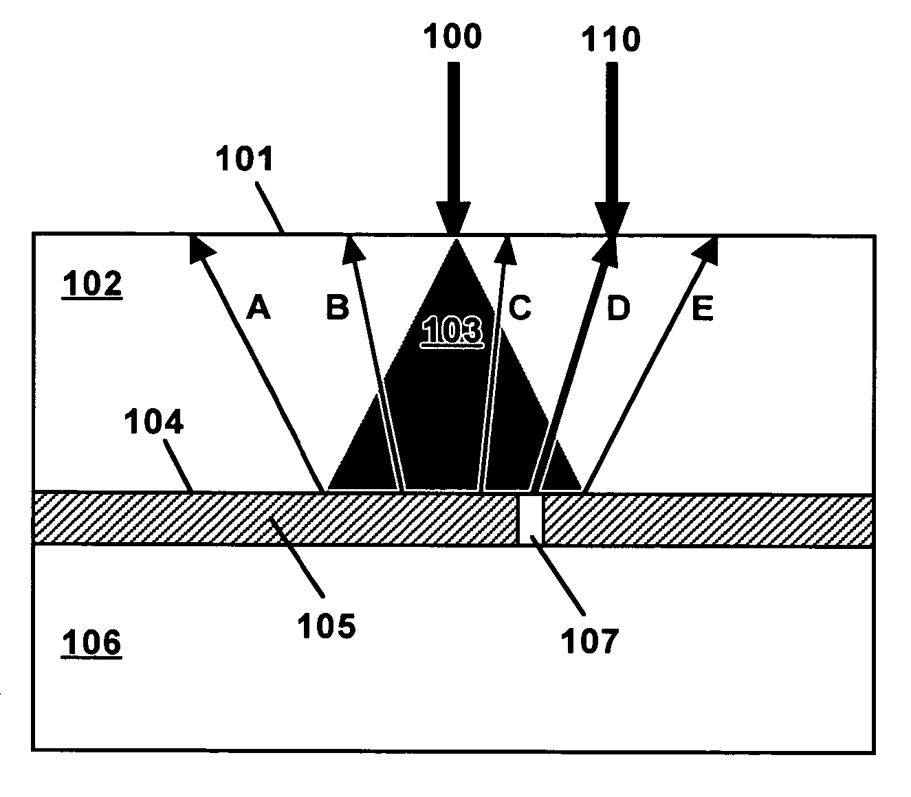
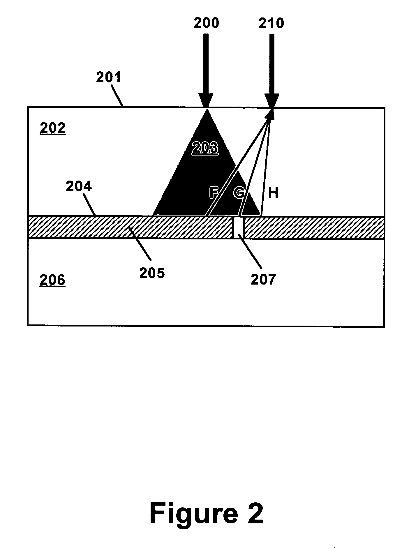
[0023] The present invention provides a laser-ultrasonic method and device that are useful for detection of defects in the underfill and solder ball attachments between a flip chip and a substrate. A flip chip includes an area array of solder balls between contact pads on the flip chip and contact pads on the substrate. The solder ball attachment is typically made by reflow soldering. The substrate may comprise any polymer-based material, FR4 material, for example, or any ceramic material, alumina, for example. The present invention may be applied to detection of attachment defects for flip chips comprising any semiconductor material, including silicon, germanium, gallium arsenide, indium phosphide, and silicon carbide. Attachment defects that may be detected include underfill voids, underfill disbonds, missing solder balls, disbanded solder balls, and solder balls with insufficient solder mass.

[0024] In this document, the term “flip chip” is used in the broadest sense and includes...


PUM


Abstract

Underfill voids and solder ball defects are detected via laser generation and laser detection of an ultrasonic wave at the top surface of flip chips. High resolution is provided by using small laser spot sizes and closely-spaced laser beams of wavelengths that are absorbed near the surface of the semiconductor. Alternatively, the generation laser beam may be absorbed in the bulk of the semiconductor. Improved spatial resolution and rejection of unwanted scattered waves can be attained by limiting the time frame of the ultrasonic waveform to the time required for the first longitudinal wave reflection from the bottom of the flip chip. The laser beam spacing can be reduced by using overlapping probe and detection beams of different wavelengths. Resolution of less than 100 μm features was demonstrated for silicon flip chips.

Description

U.S. GOVERNMENT RIGHTS [0001] This invention was made with Government support under Contract No. DTRA01-03-C-0030 awarded by the Missile Defense Agency. The Government has certain rights in this invention.BACKGROUND OF THE INVENTION [0002] 1. Field of the Invention [0003] The present invention is generally related to electronics assembly and is more specifically concerned with quality control of flip chip attachment. [0004] 2. Description of the Related Art [0005] Modern electronic assemblies generally contain integrated circuits and digital memory incorporated in semiconductor chips. In early approaches, chips were mounted and contacted electrically via wire bonds running from metallic contact pads around the periphery of the top side of the chip to mating pads on a polymer-based or ceramic chip carrier or substrate. The carrier and chip were typically contained in a package that protected the chip, and had solderable leads for attachment to a circuit board. Later approaches involv...

Claims


Application Information

Patent Timeline
IPC IPC(8): G01N29/04G01N29/00G01V13/00G01H5/00
CPCG01H9/00G01N29/11G01N29/2418G01N2291/0235G01V11/00G01N2291/0422G01N2291/044G01N2291/2672G01N2291/0421
Inventor KLEIN, MARVINMURRAY, TODD
Owner OPTECH VENTURES
Why Eureka
Try Eureka