Method for fabricating semiconductor device

a semiconductor device and manufacturing method technology, applied in the field of semiconductor device manufacturing methods, can solve the problems of changing the program state of the cell, degrading the data retention capability of the device, and failing to obtain desired device characteristics, so as to prevent the degradation of the data retention capability of the memory cell, improve the reliability of the semiconductor device, and prevent the threshold voltage failure of the memory cell.

Active Publication Date: 2006-02-16
PANNOVA SEMIC
View PDF5 Cites 8 Cited by
  • Summary
  • Abstract
  • Description
  • Claims
  • Application Information

AI Technical Summary

Benefits of technology

[0022] With the first method for fabricating a semiconductor device, when the electrode (word line) of a conductive film is formed over the trapping film, the insulating film hinders the edges of the trapping film from coming into direct contact with the electrode. Therefore, even if ion implantation damages the upper surfaces of the edges of the trapping film to reduce those upper surfaces in thickness, a silicon nitride film which is a substantial charge accumulation layer of the trapping film does not come into direct contact with the electrode. This prevents degradation in the data retention capability of the memory cell. As a result of this, the reliability of the semiconductor device can be improved. Moreover, in the step (d) of forming insulating oxide films in upper portions of the diffused layers, the insulating film is subjected to reoxidation (baking). Therefore, unlik

Problems solved by technology

The inventors made various studies and then found that the above-described conventional method for fabricating a nonvolatile semiconductor memory device causes a problem of failing to obtain desired device characteristics due to damages to the ends of the tra

Method used


Image

  • Method for fabricating semiconductor device
  • Method for fabricating semiconductor device
  • Method for fabricating semiconductor device

Examples


first embodiment

(First Embodiment)

[0047] A first embodiment of the present invention will be described with reference to the accompanying drawings.

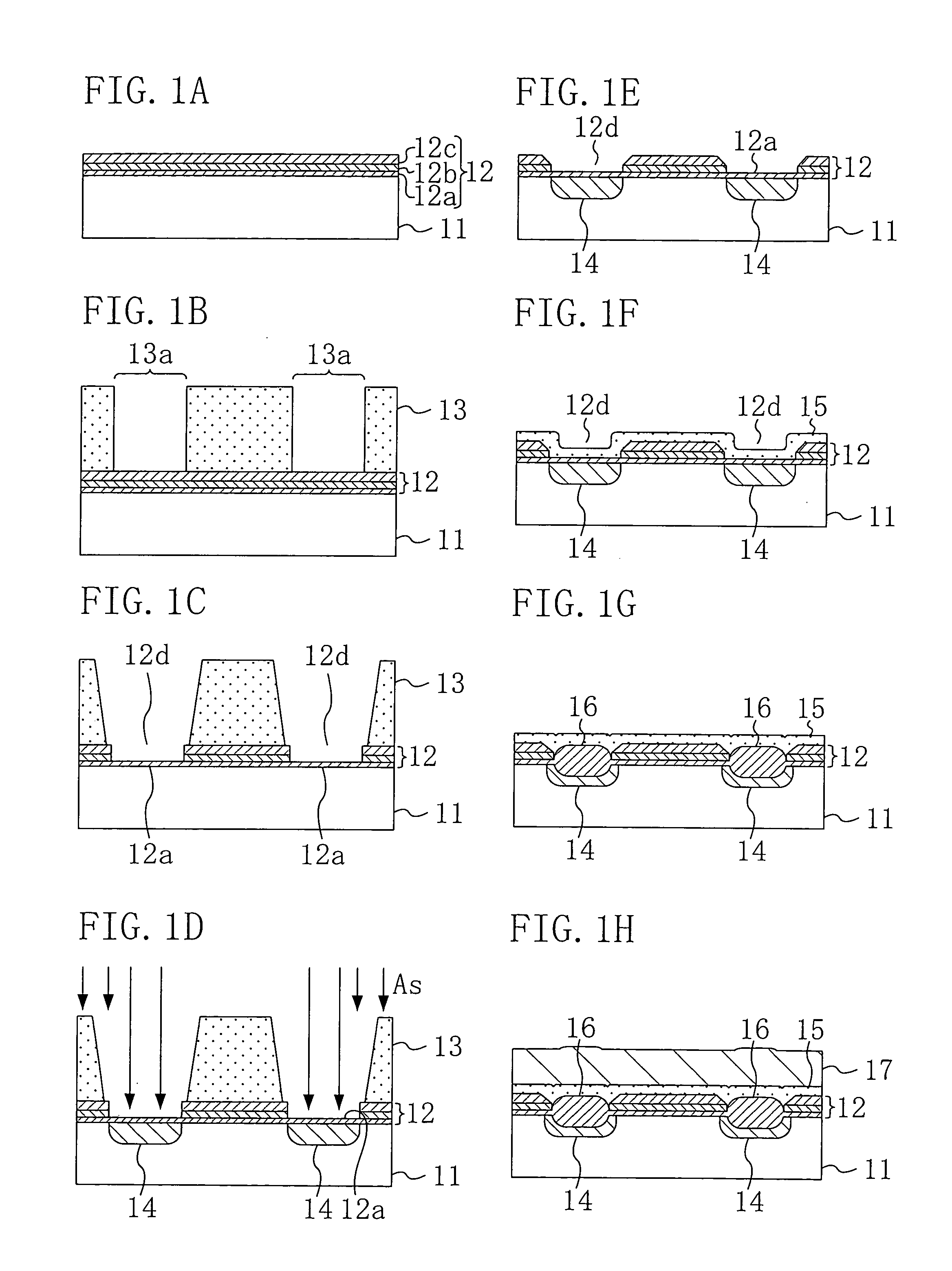
[0048]FIGS. 1A to 1H show sectional structures of a semiconductor device in the order of process steps of a method for fabricating the device according to the first embodiment of the present invention.

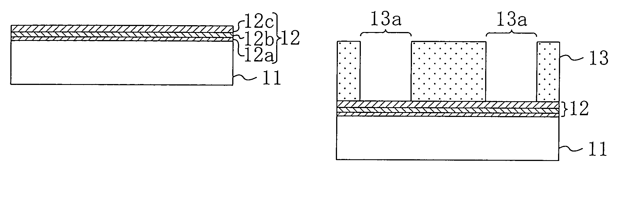
[0049] Referring to FIG. 1A, first, a principal surface of a semiconductor substrate 11 made of p-type silicon (Si) is thermally oxidized in an oxidizing atmosphere at, for example, about 1000° C., thereby forming, on the principal surface of the semiconductor substrate 11, a first silicon dioxide (SiO2) film 12a with a thickness of about 5 nm. Then, for example, by a low pressure chemical vapor deposition (LP-CVD) method with a deposition temperature of about 700° C., a silicon nitride (SiN) film 12b with a thickness of about 15 nm is deposited on the first silicon dioxide film 12a. The deposited silicon nitride film 12b is thermally oxidized in an oxidi...

second embodiment

(Second Embodiment)

[0063] A second embodiment of the present invention will be described below based on the accompanying drawings.

[0064]FIGS. 4A to 4K show sectional structures of a semiconductor device in the order of process steps of a method for fabricating the device according to the second embodiment of the present invention.

[0065] Referring to FIG. 4A, first, a principal surface of a semiconductor substrate 11 made of p-type silicon is thermally oxidized in an oxidizing atmosphere at a temperature of, for example, about 1000° C., thereby forming, on the principal surface of the semiconductor substrate 11, a first silicon dioxide film 12a with a thickness of about 5 nm. Then, for example, by a low-pressure CVD method with a deposition temperature of about 700° C., a silicon nitride (SiN) film 12b with a thickness of about 20 nm is deposited on the first silicon dioxide film 12a. The deposited silicon nitride film 12b is thermally oxidized in an oxidizing atmosphere at about 1...

third embodiment

(Third Embodiment)

[0081] A third embodiment of the present invention will be described below based on the accompanying drawings.

[0082]FIGS. 6A to 6H shows sectional structures of a semiconductor device in the order of process steps of a method for fabricating the device according to the third embodiment of the present invention.

[0083] Referring to FIG. 6A, first, a principal surface of a semiconductor substrate 11 made of p-type silicon is thermally oxidized in an oxidizing atmosphere at, for example, about 1000° C., thereby forming, on the principal surface of the semiconductor substrate 11, a first silicon dioxide film 12a with a thickness of about 5 nm. Then, for example, by a low-pressure CVD method with a deposition temperature of about 700° C., a silicon nitride (SiN) film 12b with a thickness of about 20 nm is deposited on the first silicon dioxide film 12a. The deposited silicon nitride film 12b is thermally oxidized in an oxidizing atmosphere at about 1000° C. to form, on...


PUM


Abstract

First, on a semiconductor region of a first conductivity type, a trapping film is formed which stores information by accumulating charges. Then, the trapping film is formed with a plurality of openings, and impurity ions of a second conductivity type are implanted into the semiconductor region from the formed openings, thereby forming a plurality of diffused layers of the second conductivity type in portions of the semiconductor region located below the openings, respectively. An insulating film is formed to cover edges of the trapping film located toward the openings, and then the semiconductor region is subjected to a thermal process in an atmosphere containing oxygen to oxidize upper portions of the diffused layers. Thereby, insulating oxide films are formed in the upper portions of the diffused layers, respectively. Subsequently, a conductive film is formed over the trapping film including the edges thereof to form an electrode.

Description

CROSS-REFERENCE TO RELATED APPLICATIONS [0001] This application claims priority under 35 U.S.C. § 119 on Patent Application No. 2004-236714 filed in Japan on Aug. 16, 2004, the entire contents of which are hereby incorporated by reference. BACKGROUND OF THE INVENTION [0002] (a) Fields of the Invention [0003] The present invention relates to methods for fabricating a semiconductor device. In particular, the present invention relates to methods for fabricating a semiconductor device which includes a trapping film for charge accumulation and a bit line both provided for a MONOS nonvolatile semiconductor memory device. [0004] (b) Description of Related Art [0005] MONOS (metal-oxide-nitride-oxide-semiconductor) nonvolatile semiconductor memory devices are nonvolatile semiconductor memory devices in which charges are accumulated in an ONO film of a stacked structure made by sequentially stacking silicon oxide, silicon nitride, and silicon oxide. Until now, various types of MONOS nonvolati...

Claims


Application Information

Patent Timeline
IPC IPC(8): H01L21/84H01L21/00
CPCH01L27/11568H01L27/115H10B43/30H10B69/00
Inventor YOSHIDA, KOJITAKAHASHI, KEITANORO, FUMIHIKOARAI, MASATOSHITAKAHASHI, NOBUYOSHI
Owner PANNOVA SEMIC
Why Eureka
Try Eureka