

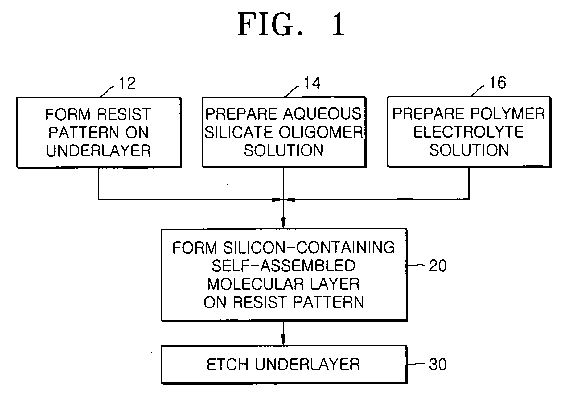
Mask pattern for semiconductor device fabrication, method of forming the same, and method of fabricating finely patterned semiconductor device
a semiconductor device and mask pattern technology, applied in the field of mask pattern for semiconductor device fabrication, can solve the problems of difficult to form contact holes less than 150 nm in size, short-wavelength exposure tool based lithography has many difficulties, and mask formation technology and resolution is not easy to achieve, and achieves simple method and simple and inexpensive process. , the effect of reducing the cd of the opening
- Summary
- Abstract
- Description
- Claims
- Application Information
AI Technical Summary
Benefits of technology
Problems solved by technology
Method used
Image

Examples
example 1
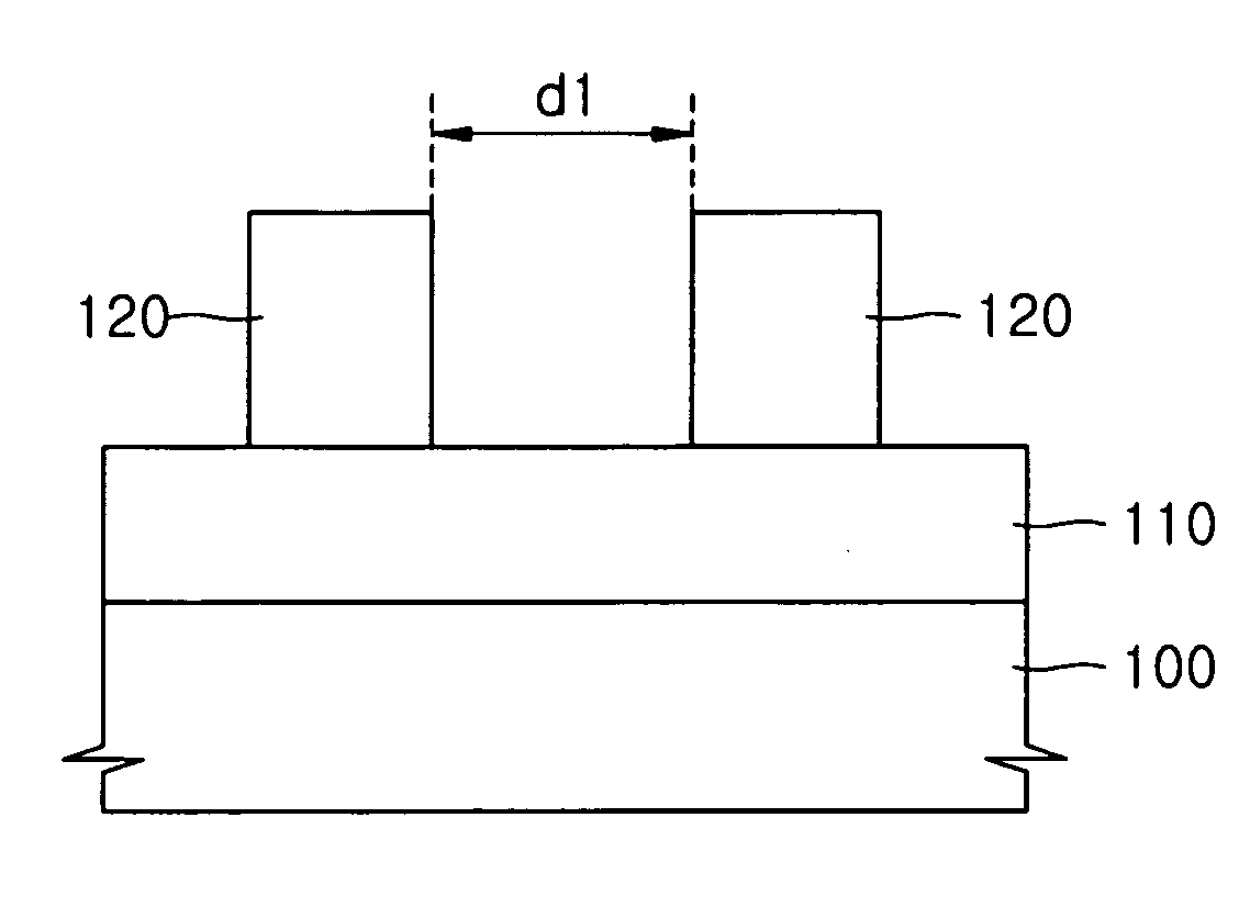
[0146] An organic antireflection film (DUV-30, Nissan Chemical Industries, Ltd.) was formed to a thickness of 36 nm on a bare silicon wafer and a photoresist (SAIL-G24c, ShinEtsu Chemical Co. Ltd.) was coated thereon to form a resist film with a thickness of 240 nm. The wafer, on which the resist film was formed, was subjected to soft baking, followed by exposure with ArF (193 nm) stepper (ASML 1100) specified with numeric aperture (NA) of 0.75 (annular illumination: 0.85-0.55) and 23 mJ / cm2 exposure light energy, and post-exposure baking (PEB). Then, the wafer was developed with a 2.38 wt % tetramethylammonium hydroxide (TMAH) solution to form, on the wafer, a resist pattern with openings defining a hole pattern with CD (critical dimension) of 112.9 nm.
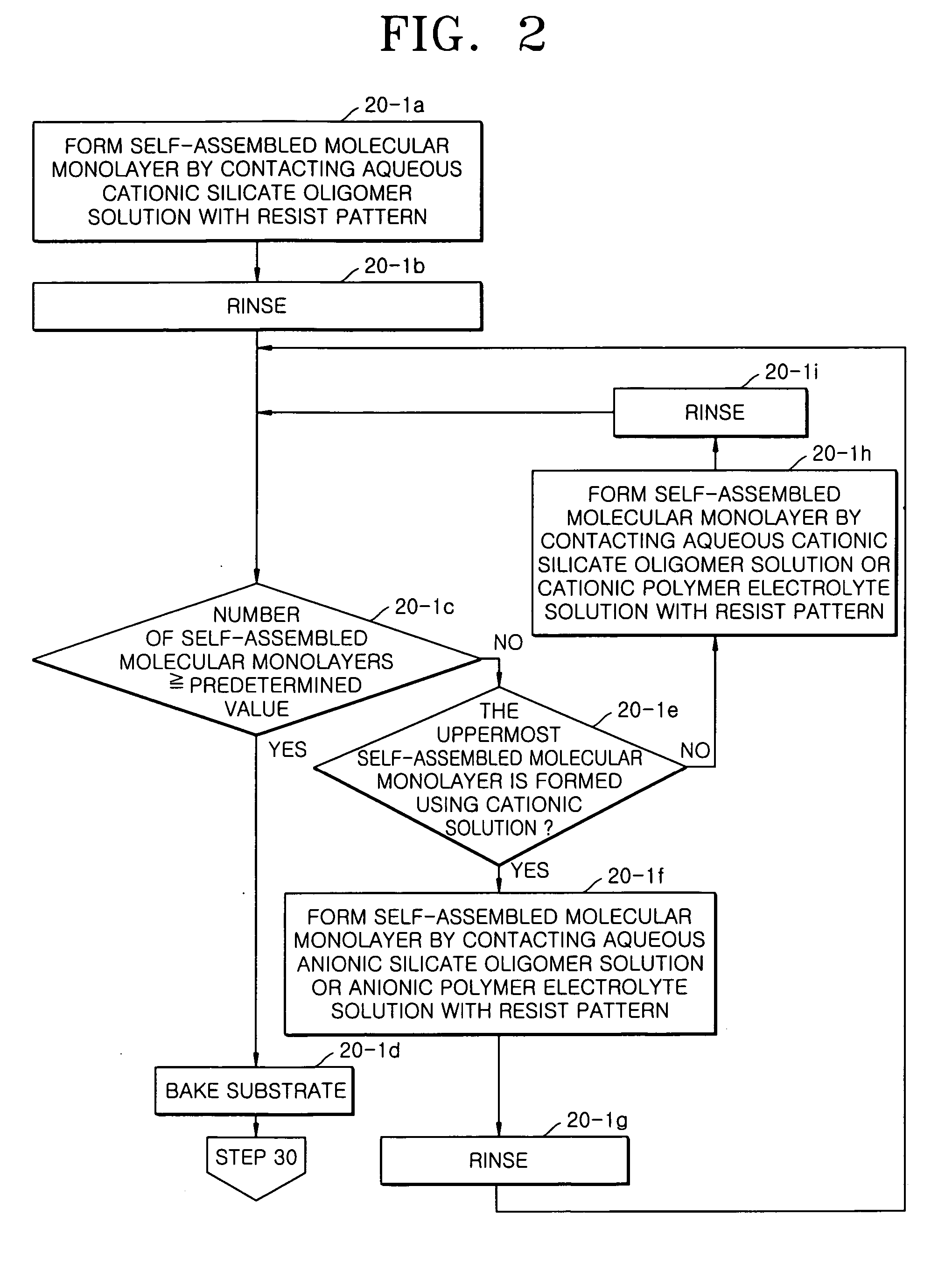
[0147] 20 ml of a cationic polymer electrolyte solution containing 1% poly(diallyldimethylammonium chloride) was poured onto the resist pattern and puddled for 30 seconds. Then, the wafer was rinsed with deionized water.
[0148] 20 m...
example 2
[0149] 20 ml of a cationic polymer electrolyte solution containing 1% poly(diallyldimethylammonium chloride) was poured onto the mask pattern obtained in Example 1 and puddled for 30 seconds. Then, the wafer was rinsed with deionized water.
[0150] 20 ml of an aqueous anionic silicate oligomer solution prepared from 1% tetraethyl orthosilicate and 60 ppm sodium hydroxide was poured onto the wafer and puddled for 30 seconds. Then, the wafer was rinsed with deionized water.
[0151] 20 ml of a cationic polymer electrolyte solution containing 1% poly(diallyldimethylammonium chloride) was poured onto the mask pattern and puddled for 30 seconds. Then, the wafer was rinsed with deionized water.
[0152] 20 ml of an aqueous anionic silicate oligomer solution prepared from 1% tetraethyl orthosilicate and 60 ppm sodium hydroxide was poured onto the wafer and puddled for 30 seconds. Then, the wafer was rinsed with deionized water to obtain a mask pattern with openings defining a hole pattern with ...
example 3
[0153]20 ml of a cationic polymer electrolyte solution containing 1% poly(diallyldimethylammonium chloride) was poured onto the mask pattern obtained in Example 2 and puddled for 30 seconds. Then, the wafer was rinsed with deionized water.
[0154] 20 ml of an aqueous anionic silicate oligomer solution prepared from 1% tetraethyl orthosilicate and 60 ppm sodium hydroxide was poured onto the wafer and puddled for 30 seconds. Then, the wafer was rinsed with deionized water to obtain a mask pattern with openings defining a hole pattern with smaller CD of 81.8 nm.
[0155] The mask pattern thus obtained was cured by baking at 150° C. for 60 seconds to complete a sol-gel reaction.
PUM
 Abstract
Description
Claims
Application Information