

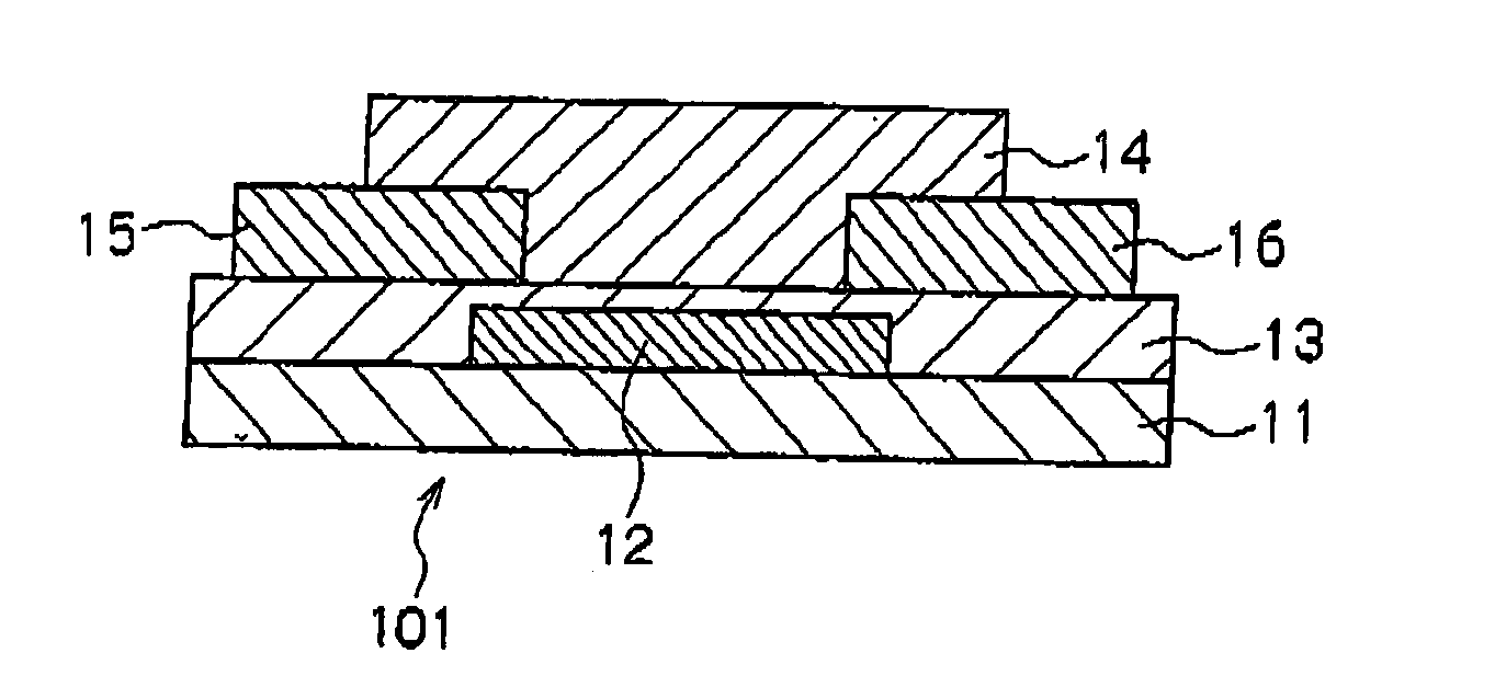
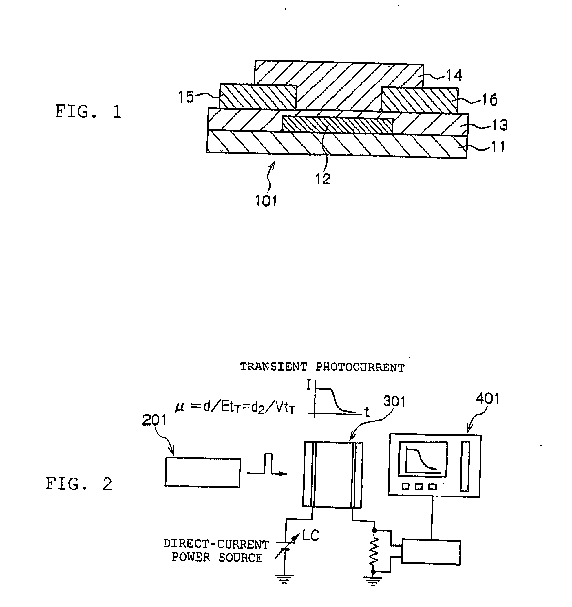
Organic semiconductor material, organic semiconductor structure, and organic semiconductor device
a technology of organic semiconductors and semiconductor layers, applied in the direction of transportation and packaging, sustainable manufacturing/processing, final product manufacturing, etc., can solve the problems of difficult formation of organic semiconductor layers, easy deformation of defects, and inability to transport charge carriers, etc., to achieve excellent processability, high charge carrier transfer properties, and high charge transport ability
- Summary
- Abstract
- Description
- Claims
- Application Information
AI Technical Summary
Benefits of technology
Problems solved by technology
Method used
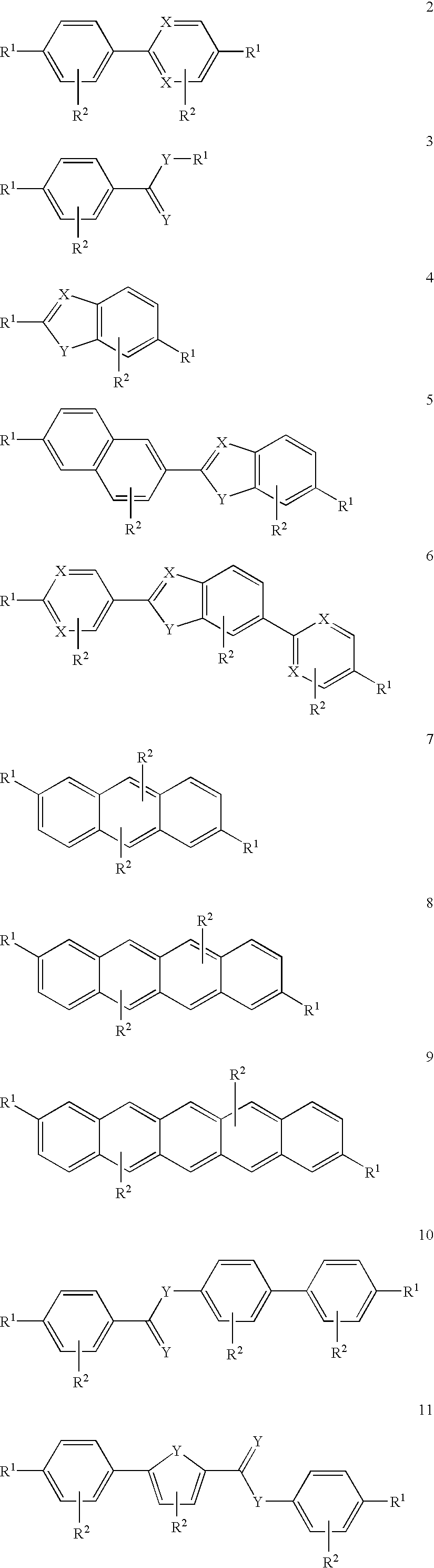
Image

Examples
examples
[0089] Hereinafter, the present invention is described in more detail showing an example of the charge transport property of low-molecular-weight and high-molecular-weight compounds having a mesogen of the same skeleton.
(Synthetic Procedure)
[0090] A suspension consisting of heptanoyl chloride (49.0 g, 0.33 mol), aluminum chloride (50.0 g, 0.375 mol) and dichloromethane (100 ml) was introduced, in an argon stream, into a 300 mL three-necked flask, and then cooled to 0° C. in an ice bath. Then, a mixed solution consisting of fluorene (24.9 g, 0.15 mol) and dichloromethane (100 ml) was dropped slowly into the suspension, over 2 hours, so that the temperature dose not become 0° C. or more. After dropping is completed, the temperature of the reaction solution was increased to room temperature, and the solution was stirred overnight. After the reaction is completed, the reaction solution exhibiting red color was poured slowly into iced water (300 ml). An organic layer of dichloromethan...
PUM
| Property | Measurement | Unit |
|---|---|---|
| electron mobility | aaaaa | aaaaa |
| temperature | aaaaa | aaaaa |
| width | aaaaa | aaaaa |
Abstract
Description
Claims
Application Information