Eureka AIR delivers breakthrough ideas for toughest innovation challenges, trusted by R&D personnel around the world.

Resonant cavity light emitting devices and associated method

a technology of light-emitting devices and resonance cavities, which is applied in the direction of crystal growth process, sub-protective fluid, semiconductor lasers, etc., can solve the problems of reducing efficiency, -scattering loss, and difficult to fabricate reliable resonant cavity devices

Inactive Publication Date: 2006-06-08
SORAA
View PDF22 Cites 308 Cited by
  • Summary
  • Abstract
  • Description
  • Claims
  • Application Information

AI Technical Summary

Benefits of technology

[0016] In one embodiment, a method may provide a resonant cavity light emitting device. A seed metal nitride crystal and a source material may be arranged in a nitrogen-containing superheated fluid disposed in a sealed container disposed in a multiple-zone furnace. Metal nitride material may be grown on the seed crystal by mass transport from the source material to the seed crystal through the nitrogen-containing superheated fluid. Said growing produces a single-crystal metal nitride substrate secured to the seed crystal. Said growing may include applying a temporally and / or spatially varying thermal gradient between the seed crystal and the source material to produce an increasing growth rate during at least a portion of the growing. A stack of group III-nitride layers may deposit on the single-crystal metal nitride substrate. The stack may include a first mirror sub-stack and an active region adapted for fabrication into one or more resonant cavity light emitting devices.

Problems solved by technology

The use of phosphors, such as in a polymer matrix, may generate light of additional wavelengths, but may have reduced efficiency by, for example, Stokes shifts, reflective or light-scattering losses, and device failures associated with the phosphor packaging.
Resonant cavity devices may provide more efficient light extraction, but it may be difficult to fabricate reliable resonant cavity devices in the group III-nitride material system.
In spite of these well-known advantages, commercial group III-nitride light emitting devices continue to be grown heteroepitaxially on sapphire or silicon carbide substrates due to a lack of high quality large-area gallium nitride substrates.
The chemical passivity of nitrogen, a high melting temperature of gallium nitride, and other factors have heretofore made growth of a large volume and high quality gallium nitride boule problematic.
The high n-type background causes substantial crystal opacity, for example optical absorption coefficients of around 200 cm−1 in the visible range, which may be problematic for flip-chip light emitters, and causes the lattice constant to increase by about 0.01 percent to about 0.02 percent, generating strain in epitaxial GaN layers deposited thereupon.
The undoped GaN substrates formed by this method have a carrier mobility of about 30 to about 90 cm2 / V-s, which may be problematic in high-power devices.
Repeated application of epitaxial lateral overgrowth may not be expected to suppress the tilt boundaries.
Thus, epitaxial lateral overgrowth may not be upwardly scalable in the lateral wafer dimension, and usable growth dimensions may be limited to about the order of the spacings of the nucleation openings.
Furthermore, ELO does not produce a three-dimensional single-crystal boule, and the processing involved in producing each ELO gallium nitride wafer may be labor-intensive, making automation of the ELO wafer formation process difficult.
However, these references focus on thin GaN epitaxial layers rather than bulk crystals and do not relate to resonant cavity devices.
However, the disclosed laser structure employs only a single cavity and has no capability for directional emission of two or more visible wavelengths of light or of white light.

Method used


Image

  • Resonant cavity light emitting devices and associated method
  • Resonant cavity light emitting devices and associated method
  • Resonant cavity light emitting devices and associated method

Examples


Embodiment Construction

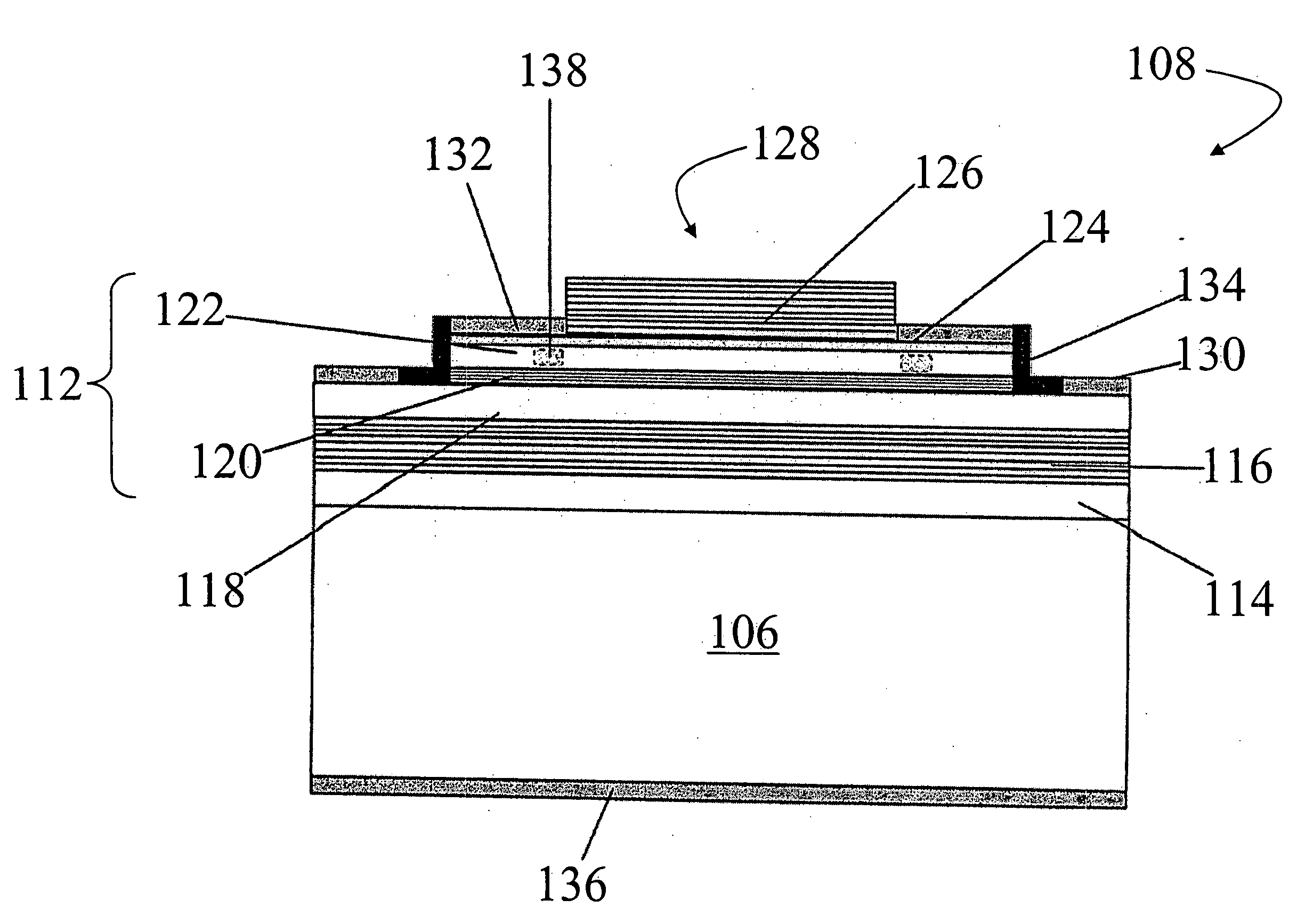
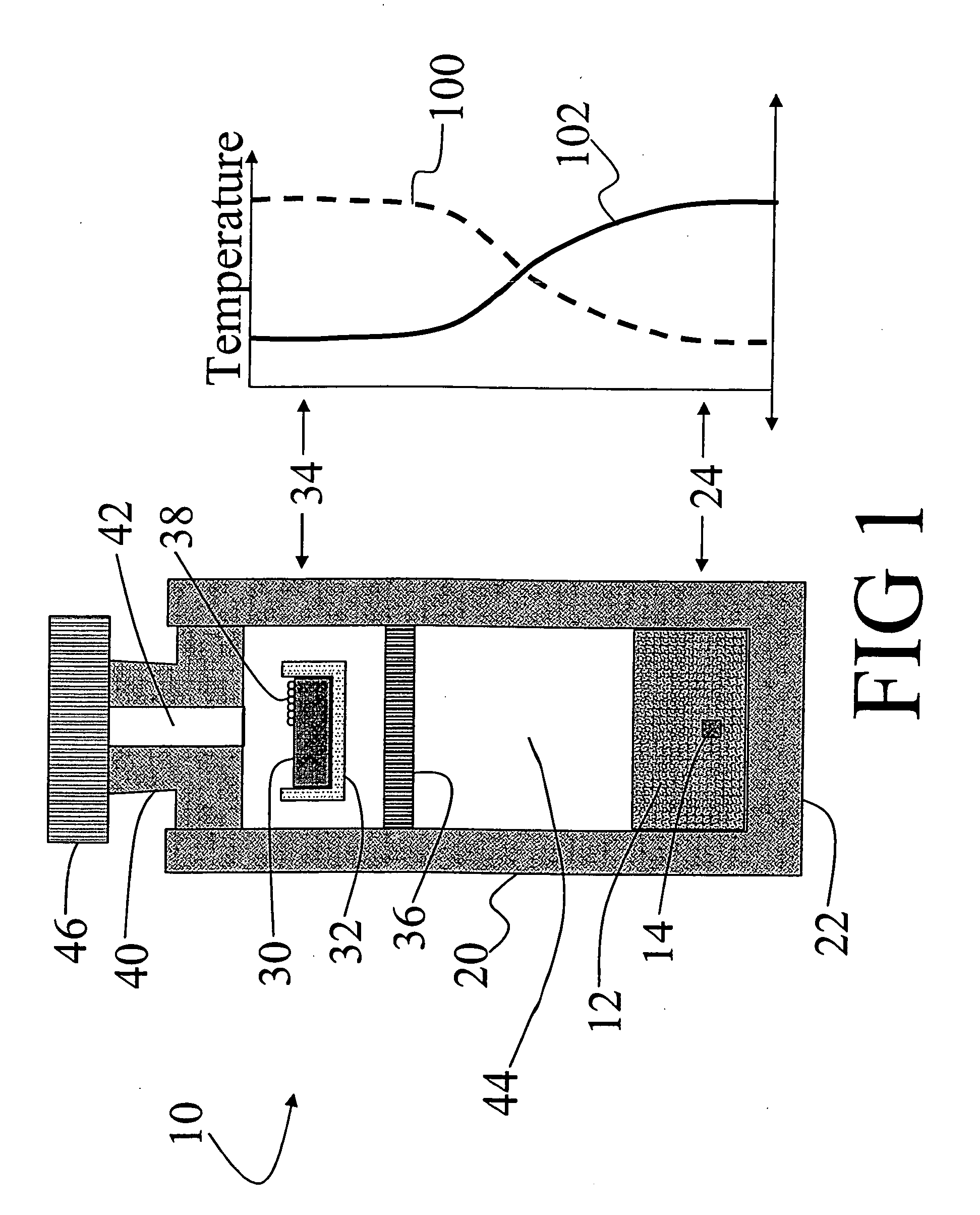
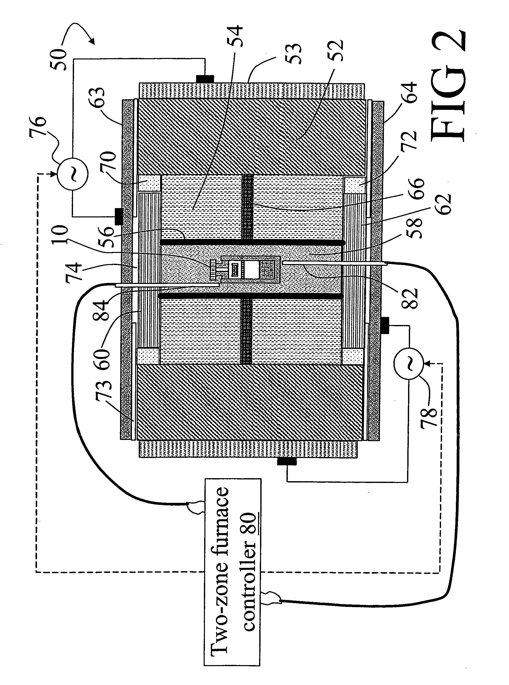
[0035] The invention may include embodiments that may relate to resonant cavity light emitting devices. The invention may include embodiments that may relate to a method of making and / or using resonant cavity light emitting devices, or components thereof.

[0036] Approximating language, as used herein throughout the specification and claims, may be applied to modify any quantitative representation that could permissibly vary without resulting in a change in the basic function to which it is related. Accordingly, a value modified by a term such as “about” is not to be limited to the precise value specified, and may include values that differ from the specified value. In at least some instances, the approximating language may correspond to the precision of an instrument for measuring the value. Similarly, “free” may be used in combination with a term, and may include an insubstantial number, or trace amounts, while still being considered free of the modified term.

[0037] With reference...


PUM

PropertyMeasurementUnit
dislocation densityaaaaaaaaaa
optical absorption coefficientsaaaaaaaaaa

Abstract

A method may produce a resonant cavity light emitting device. A seed gallium nitride crystal and a source material in a nitrogen-containing superheated fluid may provide a medium for mass transport of gallium nitride precursors therebetween. A seed crystal surface may be prepared by applying a first thermal profile between the seed gallium nitride crystal and the source material. Gallium nitride material may be grown on the prepared surface of the seed gallium nitride crystal by applying a second thermal profile between the seed gallium nitride crystal and the source material while the seed gallium nitride crystal and the source material are in the nitrogen-containing superheated fluid. A stack of group III-nitride layers may be deposited on the single-crystal gallium nitride substrate. The stack may include a first mirror sub-stack and an active region adaptable for fabrication into one or more resonant cavity light emitting devices.

Description

CROSS REFERENCE TO RELATED APPLICATIONS [0001] This application may be a continuation-in-part of application Ser. No. 10 / 693,803, filed Oct. 24, 2003, and claims benefit therefrom, the contents of which may be incorporated by reference in their entirety.BACKGROUND [0002] 1. Technical Field [0003] The invention may include embodiments that may relate to resonant cavity light emitting devices. The invention may include embodiments that may relate to a method of making and / or using resonant cavity light emitting devices, or components thereof. [0004] 2. Discussion of Related Art [0005] Light may be extracted from a light emitting diode (LED). The light emitting diode may emit light of only one wavelength, whereas for many applications at least one additional wavelength or white light may be desirable. The use of phosphors, such as in a polymer matrix, may generate light of additional wavelengths, but may have reduced efficiency by, for example, Stokes shifts, reflective or light-scatte...

Claims


Application Information

Patent Timeline
Patent Type & Authority Applications(United States)
IPC IPC(8): H01L33/00C30B9/00H01L33/10
CPCC30B9/00C30B29/403Y10T117/1064H01L33/007H01L33/105C30B29/406H01S5/187H01S5/323
Inventor D'EVELYN, MARK PHILIPCAO, XIAN-ANZHANG, ANPINGLEBOEUF, STEVEN FRANCISHONG, HUICONGPARK, DONG-SILNARANG, KRISTI JEAN
Owner SORAA
Why Eureka
Eureka Blog
Learn More