
Lightly doped silicon carbide wafer and use thereof in high power devices

a technology of silicon carbide wafers and silicon carbide wafers, which is applied in the direction of crystal growth process, basic electric elements, electrical apparatus, etc., can solve the problems of high cost of layers thicker than 100 m, low growth rate, and limited ability of these switching devices to handle higher voltages

Active Publication Date: 2006-06-29
SICED ELECTRONICS DEV +1
View PDF5 Cites 33 Cited by
  • Summary
  • Abstract
  • Description
  • Claims
  • Application Information

AI Technical Summary

Benefits of technology

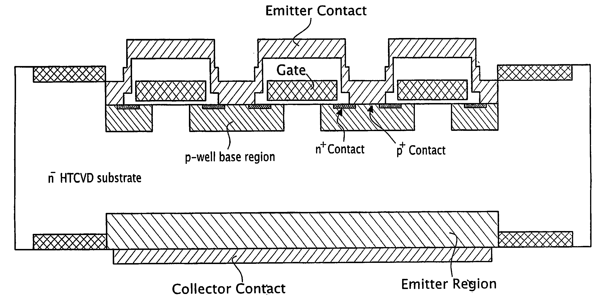
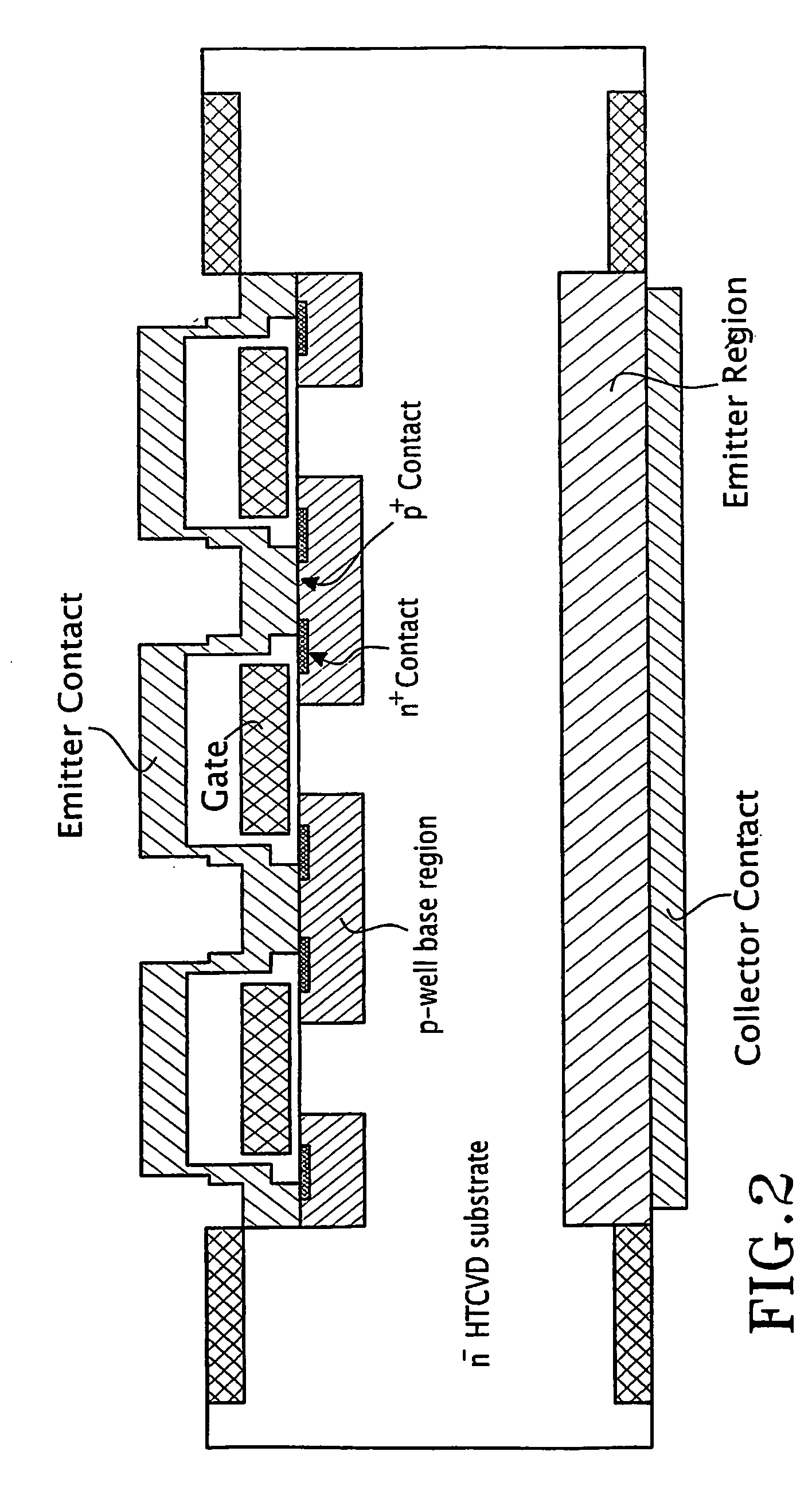
[0012] The most important advantage of the invention is the possibility to fabricate a semiconductor structure without a low resistivity substrate, which in the case of a vertical power device represents only an unnecessary additional resistance. The whole wafer consists now of a low doped n-drift zone (FIG. 2) able to block very high voltages (larger than 15 kV).
is the possibility to fabricate a semiconductor structure without a low resistivity substrate, which in the case of a vertical power device represents only an unnecessary additional resistance. The whole wafer consists now of a low doped n-drift zone (FIG. 2) able to block very high voltages (larger than 15 kV).

Problems solved by technology

The ability of these switching devices to handle higher voltages is today limited by technological factors, such as requirements of serial operations, and by the physical properties of the silicon semiconductor.
The main disadvantage of the CVD process lies in its low growth rate and thus high cost for layers thicker than 100 μm.
This technology presently limits silicon power devices to voltage handling capabilities to the 10 kV range.
This approach can however not be used with the present state-of-the-art silicon carbide wafers due to the lack of lightly doped, microsecond range lifetime, SiC wafers.
The incorporation of aluminum is hard to control in sublimation growth furnaces especially in the case of high doping concentrations.
Thus, it is not possible to fabricate an attractive IGBT like structure using a p-type substrate with a n-type drift zone grown by epitaxy.
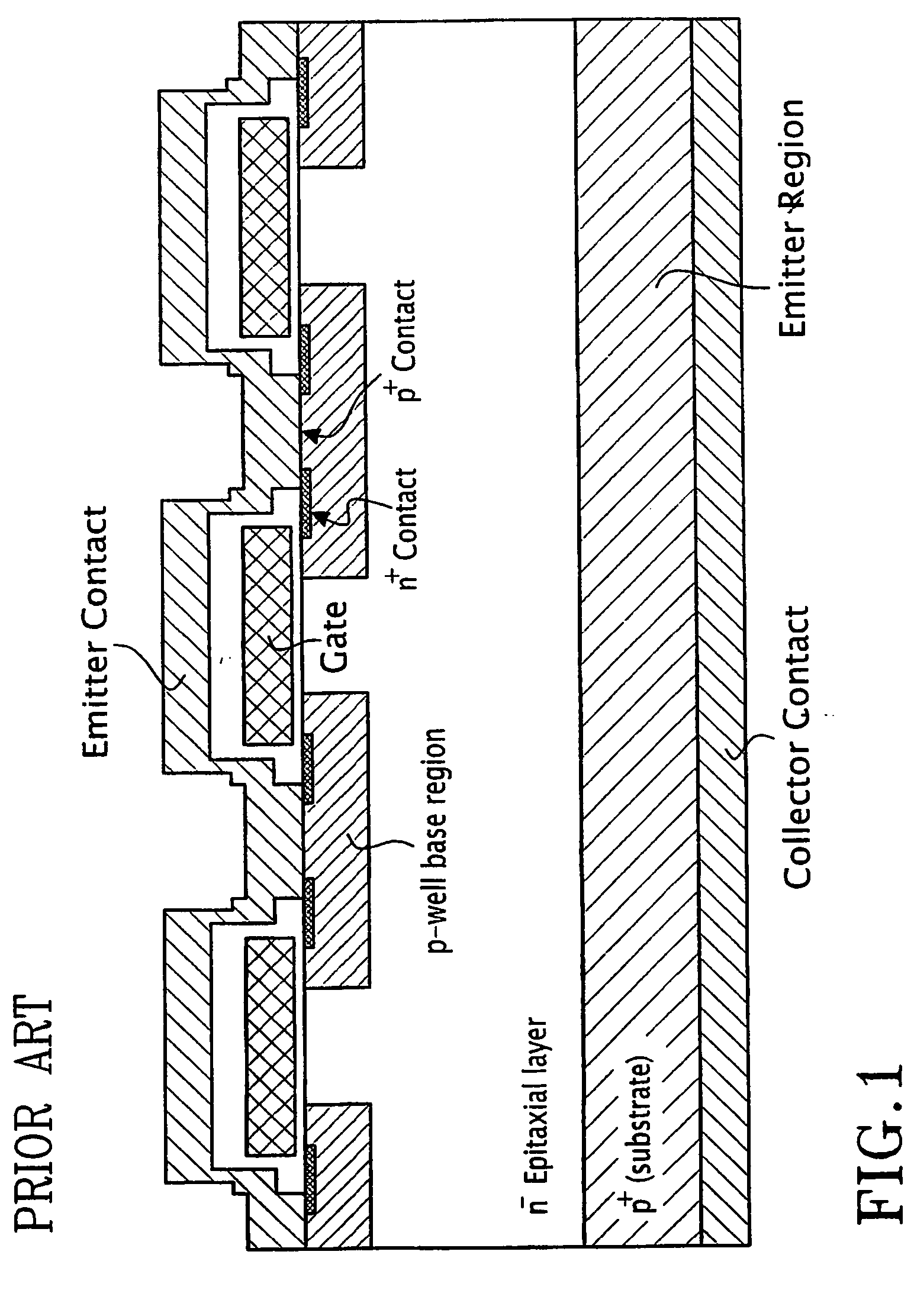
Additionally, also assuming the availability of a suited base material, there are only restricted possibilities to adjust device parameters by lifetime modulation near the backward emitter of a deduced IGBT structure (FIG. 1).
Up to know, the realized IBGT structures on epitaxied SiC substrates suffer from unsatisfactory technical parameters.
The successful realization of a classical IGBT structure using a MOS Gate seems not to be possible, since in this case the oxide stress is very high and the reliability will be strongly degraded (except using adequate shielding precautions).

Method used


Image

  • Lightly doped silicon carbide wafer and use thereof in high power devices
  • Lightly doped silicon carbide wafer and use thereof in high power devices
  • Lightly doped silicon carbide wafer and use thereof in high power devices

Examples


example 1

[0043] A SiC single crystal of the 4H polytype was grown in a HTCVD furnace with an average growth rate of 400 μm / h. A small nitrogen flow was added to the silane, ethylene and carrier gas flows fed into the furnace to provide a light n-type doping. Wafers were sliced and polished from this crystal and analysed using the Capacitance-Voltage (C-V), Deep Level Transient Spectroscopy (DLTS), Secondary Ion Mass Spectroscopy (SIMS) and Time Resolved Photoluminescence (TRPL) techniques. The CV and DLTS measurements were identified as not being possible to perform on these wafers due to compensation of the nitrogen donors by at least one deep level. SIMS measurements revealed a Ti contamination at a concentration of 3×1015 cm−3, whereas other impurities such as B, Al and V had at least one order of magnitude lower concentration. TRPL measurements performed on such wafers, either after polishing or after annealing at 1600° C. for 1 hour, showed a decay time less than the detection limit of ...

example 2

[0044] The growth system was modified to suppress Ti contamination into the growing crystal by selecting components preventing release of unwanted impurities, such as transition metals, into the growth atmosphere. A low-doped n-type 4H SiC crystal was grown In conditions comparable to those in the previous example. The Ti concentration in this crystal was decreased to 5×1013 cm−3. DLTS measurements on as-polished wafers from this crystal showed however the presence of deep levels located at about 0.66 eV and about 1,5 eV from the conduction band with concentrations of 4,5×1015 cm−3 and 3×1015 cm−3, respectively (FIG. 5). The carrier lifetime, measured by TRPL on the same substrate, was less than 5 ns. The wafer was subsequently annealed for 1 hour at a temperature of 1600° C. in a hydrogen ambient. The concentration of the deep levels identified by DLTS in the as-polished wafers was drastically reduced after the annealing (FIG. 5). TRPL measurement also showed that recombination of ...

example 3

[0045] The findings of the previous examples were taken into account by modifying the growth conditions to reduce the concentration of intrinsic defects grown-in in the crystal. In this example, the input C / Si ratio of the ethylene / silane gas mixture was increased. FIG. 6 shows that wafers sliced and polished from such a crystal have a substantially lower concentration of the deep levels identified by DLTS at 1,5 eV, but a similar concentration of the Z1 / 2 level. Upon annealing at 1600° C. in either an hydrogen or an argon ambient, the concentration of both deep levels is decreased, as in the previous example (FIG. 6). The carrier lifetime of the substrate annealed in an hydrogen containing ambient was however increased by a factor 3, to ca. 60 ns (FIG. 7). The carrier lifetime of another wafer cut from the same crystal and annealed in a pure argon ambient however remained below the detection limit of the TRPL system.

[0046] It is understood that the teachings of the first embodimen...


PUM

PropertyMeasurementUnit
carrier concentrationaaaaaaaaaa
thicknessaaaaaaaaaa
thicknessaaaaaaaaaa

Abstract

A uniform silicon carbide single crystal with either an n-type or a p-type conductivity. The crystal has a net carrier concentration less than 1015 cm−3 and a carrier lifetime of at least 50 ns at room temperature.

Description

FIELD OF THE INVENTION [0001] The invention relates to [0002] a lightly doped n-type or p-type silicon carbide wafer having a sufficiently low concentration of deep levels originating from either impurities, intrinsic defects or structural defects to enable free carriers injected into such wafer to recombine with a lifetime of interest for bipolar power devices, [0003] the use of a lightly doped n- or p-type silicon carbide wafer as base region of a high power device structure such as an IGBT with a voltage blocking capability of 15 kV or more. BACKGROUND AND PRIOR ART [0004] Currently, the highest breakdown voltages achieved by silicon power devices range from 4.5 to 6.5 kV for IGBTS and GTOs, and 9 to 12 kV for thyristors. The ability of these switching devices to handle higher voltages is today limited by technological factors, such as requirements of serial operations, and by the physical properties of the silicon semiconductor. It is considered that higher voltage (>10 kV) e...

Claims


Application Information

Patent Timeline
Patent Type & Authority Applications(United States)
IPC IPC(8): C30B15/00C30B21/06C30B27/02C30B28/10C30B30/04C30B29/36C30B25/00H01L21/04H01L21/205H01L21/324H01L21/336H01L29/12H01L29/161H01L29/24H01L29/739H01L29/78
CPCC30B25/00H01L21/0455H01L29/1608H01L29/66068H01L29/7395C30B29/36Y10S438/931H01L21/02378H01L21/02433H01L21/02529H01L21/0262
Inventor ELLISON, ALEXANDREMAGNUSSON, BJORNVEHANEN, ASKOSTEPHANI, DIETRICHMITLEHNER, HEINZFRIEDRICHS, PETER
Owner SICED ELECTRONICS DEV
Learn More