Method and apparatus to reduce the jitter in wideband PLL frequency synthesizers using noise attenuation

a wideband pll frequency synthesizer and noise attenuation technology, applied in electrical equipment, transmission, automatic control, etc., can solve the problems of reducing the required silicon area, too big to be integrated on-chip, and a higher gate leakage current, so as to reduce the contribution of loop filter nois

Inactive Publication Date: 2006-06-29
SILICON LAB INC
View PDF10 Cites 58 Cited by
  • Summary
  • Abstract
  • Description
  • Claims
  • Application Information

AI Technical Summary

Benefits of technology

[0023] The present disclosures provides a novel PLL loop filter architecture that utilizes a noise attenuator between the loop filter and the controlled oscillator of the PLL, and that reduces the loop filter noise contribution and the reference and supply injected spurs. The attenuator may be considered to be a separate circuit block between the loop filter, may be implemented as a portion of the loop filter or may be implemented as a portion of the controlled oscillator. In this regard, it will be recognized that the benefits of the attenuation concepts disclosed herein for use in a PLL may be obtained regardless of what portion of the PLL circuit blocks the attenuation circuitry is classified to be contained within.
[0025] In one embodiment, a phase locked loop circuit is provided. The phase locked loop circuit may include a controllable oscillator providing an oscillator output, a loop filter coupled within a loop path of the phase locked loop and an attenuator located within the loop path. The attenuator may be located between at least a portion of the loop filter and an input of the controllable oscillator. The attenuator reduces phase noise in a clock provided at the oscillator output.

Problems solved by technology

The large PLL loop bandwidth together with the high oscillator gain makes the PLL front-end to be a significant and in some cases the dominant contributor to the output clock total phase noise (jitter).
However for a given loop bandwidth (RC time constant) a low output phase noise requires a low value series resistor (R) and therefore a large value capacitor (C) that in some applications may be too big to be integrated on-chip.
In deep-submicron CMOS processes the MOS devices come with an ever increasing capacitance density, reducing the required silicon area, but unfortunately this comes at the price of a larger gate leakage current.
This creates a large ripple on the oscillator control signal (voltage or current) and thus results in large reference spurs in the output clock spectrum.
The reference spurs are detrimental to the frequency translation PLLs due to the reciprocal mixing effect that can fold unwanted signals (blockers) on top of the wanted signal.
The main drawback of MIM capacitors is that they require extra processing steps and therefore increase the processing cost.
Another drawback is the relatively large area took by the MIM capacitors, due to their relatively low capacitance density.
The drawbacks are the larger required area (comparable with the MIM capacitors) and a poor modeling of the resulting capacitance absolute value.
Their drawback is the rather poor isolation from the substrate noise that can be coupled in the PLL loop filter, degrading the output clock jitter performance.
The parasitic substrate noise injection becomes particularly troublesome when large area capacitors are used (e.g. 10,000 um2 and higher).
In a standard passive RC filter this results in very large value loop filter capacitors (nF) that cannot be integrated on-chip.
Beside the cost penalty, large loop filter capacitors have also the drawback of an increased parasitic capacitance to the substrate and thus a higher substrate noise sensitivity.
Voltage-mode Miller multiplication has the drawback of a reduced voltage range at the output of the charge-pump, restricting the output clock frequency range.
Current-mode Miller multiplication does not present the voltage headroom problem, but requires a large current in the loop filter, thus being not suitable for portable applications.
In low noise applications the Miller gain is limited to around 5, being much less effective for the on-chip integration of the PLL loop filter.
This solution is required in the case of standard deep submicron CMOS processes that do not offer thick oxide capacitors and MIM capacitors, and that the imposed area for the design does not allow the usage of the metal interconnect capacitors.
Unfortunately, the additional charge-pump used by the leakage current compensation loop degrades the reference spur performance of the output clock.
Therefore this architecture may be successfully used in clocking frequency synthesizers for large digital circuits, but may not be recommended in frequency translation synthesizers where large reference spurs degrade the receiver sensitivity due to the reciprocal mixing effect.
The active amplifiers (voltage or current) from the feed-forward loop filter contribute additional noise to the system, reducing the benefit of the series resistor elimination.
Large delays degrade the PLL phase margin and increase the jitter transfer peaking, leading to excess phase noise in the output clock.
Ensuring a low delay results in large currents being used in the loop filter active amplifier and therefore more excess noise.

Method used


Image

  • Method and apparatus to reduce the jitter in wideband PLL frequency synthesizers using noise attenuation
  • Method and apparatus to reduce the jitter in wideband PLL frequency synthesizers using noise attenuation
  • Method and apparatus to reduce the jitter in wideband PLL frequency synthesizers using noise attenuation

Examples


second embodiment

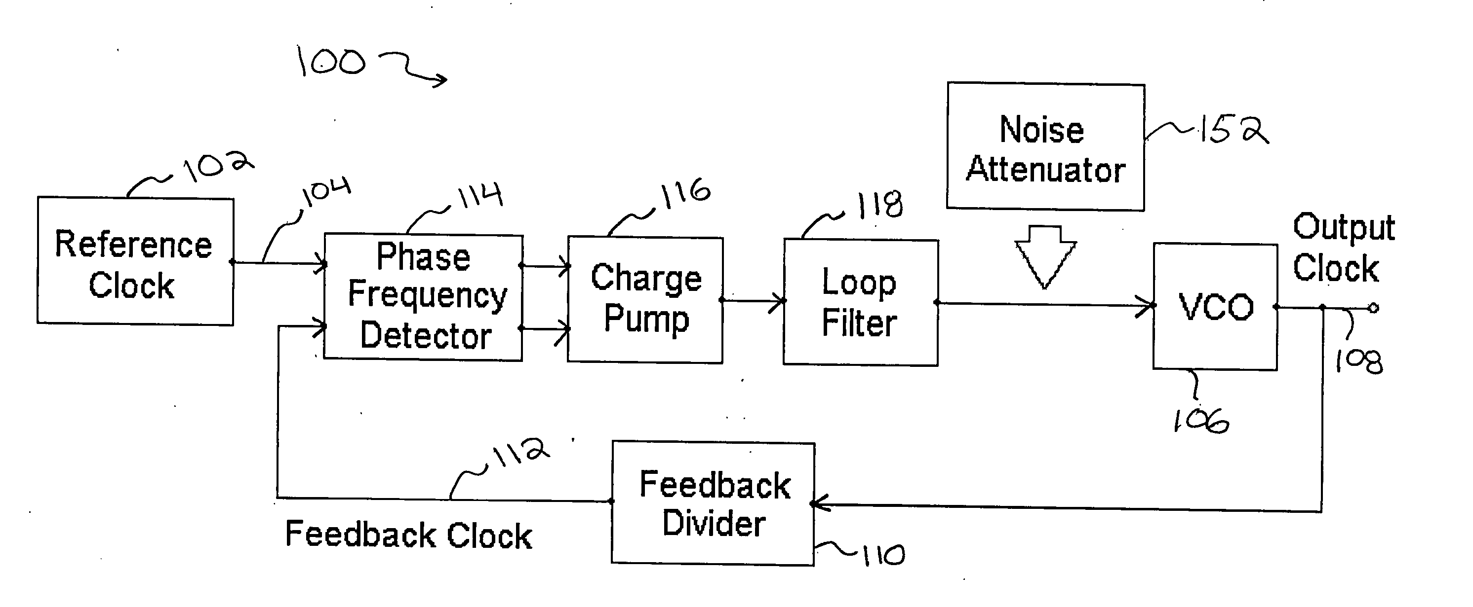
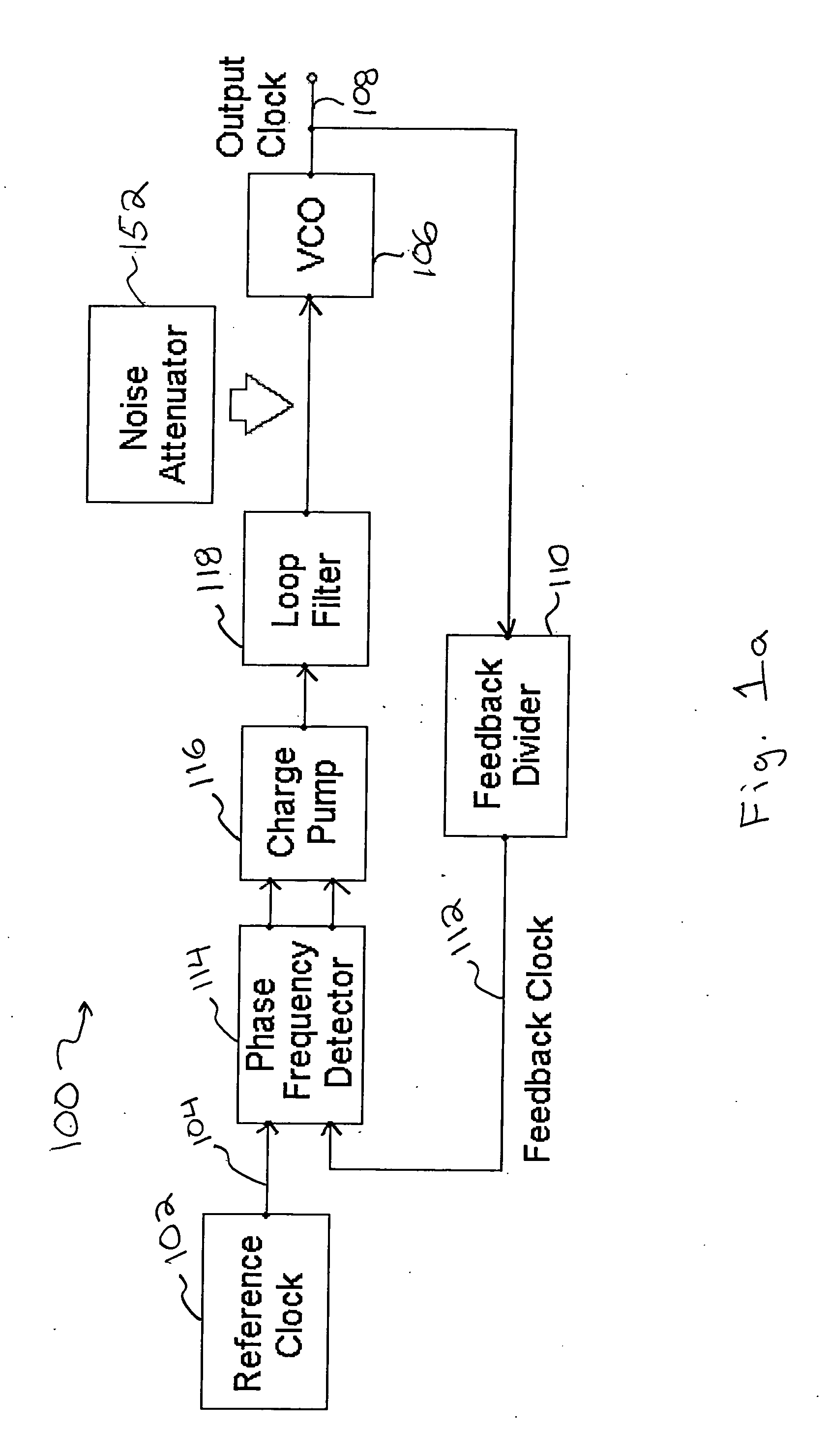
[0066] The polysilicon resistors and the transconductance of the source follower transistor do not track well over process and temperature. As a result a noticeable variation of the attenuation factor and of the output impedance may appear over process and temperature. Furthermore the control voltage for the oscillator varies over a range that has a large offset voltage (Voff; Voff+ΔV). For many oscillators the control voltage also sets the amplitude of oscillation, which needs to be kept high such that a low phase noise results. Generating the entire control voltage with an IR voltage drop leads to a large current in the attenuator, that may not be compatible with many portable applications. FIG. 3.b presents the loop filter noise attenuator in which an additional diode connected NFET Mdiod is added in the bottom leg of the divider. The transistor Mfol and diode Mdiod operate at the same current level and are in close proximity, such that they operate at the same temperature. In th...

third embodiment

[0074]FIG. 3.c presents the loop filter noise attenuator that boosts the attenuation factor by using a zero-Vt thick oxide NFET as source follower. In doing so the voltage range at the output of the charge-pump is reduced by a Vth threshold voltage for thick oxide devices (0.7-0.8V), allowing a maximum attenuation factor of 2.5 for a minimum supply voltage of 3V. As will be recognized by those skilled in the art, the embodiments shown herein are not limited to the particular device types (NFET or PFET) shown. For example, FIG. 3d illustrates a PFET version of the circuitry of FIG. 3a.

[0075] If the supply voltage has significant noise a regulator may need to be used, reducing the available headroom and thus constraining the maximum attenuation factor. It may be desirable therefore to use circuit solutions that can provide a larger value for the attenuation factor and thus a more substantial reduction of the loop filter on-chip capacitance.

c. Cascoded Source Follower Attenuator for...

first embodiment

[0111] Yet another embodiment for realizing an active attenuator is to use a common source MOSFET (or common emitter BJT) with resistive load both in the source (emitter) and drain (collector). FIG. 9a shows the common source attenuator that provides a supply referenced control voltage to the oscillator. As shown in FIG. 9a, a common source transistor Mbuf is coupled to a source resistor Rs and a drain resistor Rd.

[0112] The gain of the stage is given by the ratio of the two resistors: G=1A=-RdRS+1gm⁡(Mgain)≈-RdRS(16)

[0113] The resistor Rd is selected smaller than the resistor Rs, such that the gain results smaller than unity (attenuation). The capacitor Cp2 in conjunction with the reisistor Rd gives a second ripple pole that filters the high frequency noise. The noise of the Mbuf device (both thermal and 1 / f noise) is well degenerated by the high value resistor Rs. The noise contribution of the attenuator is dominated by the noise coming from the output resistor Rd.

[0114]FIG. 9b ...


PUM


Abstract

A noise attenuator loop filter for PLL applications that allows a full on-chip integration of the loop filter capacitors, while ensuring a low output clock phase noise (jitter) is disclosed. A voltage attenuator (A) is inserted between the loop filter (passive or active) and the controlled oscillator. The attenuator attenuates the noise coming from the loop filter. In case of a passive RC filter, the series resistor noise power is attenuated by A2 times, allowing the usage of a resistor that is A2 times larger and therefore the loop filter capacitors result A2 times smaller (easy to integrate on-chip). The relatively low value capacitor allows the usage of thick-oxide accumulation-mode MOSFET capacitors that take a reasonable low area, have a good linearity, are isolated from the substrate by the grounded N-well, and have negligible gate leakage current. Several embodiments of the noise attenuator are proposed for different practical applications: clock generation for digital circuits, frequency translation, low or high supply voltage, narrow or wide frequency range, processes with or without isolated well devices, processes with or without polysilicon resistors, and medium or high reference spurs rejection.

Description

BACKGROUND OF THE INVENTION [0001] The present invention relates to the field of phase locked loop (PLL) circuits, and more particularly to PLLs utilized in frequency synthesizers for wideband tuner applications, such as for example, satellite, cable, or terrestrial TV tuner applications. [0002] In general, a tuner is an electronic device that receives a high frequency modulated signal (e.g. satellite, cable or terrestrial TV signal) and converts it down to a much lower frequency at which the signal processing is performed. This frequency translation may be accomplished with an electronic block, a mixer, that realizes the above mentioned frequency translation usually by performing a multiplication between the input signal and a locally generated clock signal with variable frequency. The local clock is generated in most cases with frequency synthesizers. A frequency synthesizer is often a circuit block that starts from a high accuracy reference clock frequency (usually from few MHz t...

Claims


Application Information

Patent Timeline
Patent Type & Authority Applications(United States)
IPC IPC(8): H04B1/18
CPCH03L7/0891H03L7/093H03L7/18
Inventor MAXIM, ADRIANKAO, JAMES
Owner SILICON LAB INC
Why Eureka
Try Eureka