Diamond substrate and manufacturing method thereof

a technology of diamond substrate and manufacturing method, which is applied in the direction of crystal growth process, polycrystalline material growth, chemically reactive gas, etc., can solve the problems of difficult to make large-scale and maintain satisfactory crystallinity quality during chemical vapor deposition, disadvantage of productivity, and limited practical application in semiconductor and optical use. achieve the effect of convenient wafer processing

Inactive Publication Date: 2006-09-28
SUMITOMO ELECTRIC IND LTD
View PDF2 Cites 21 Cited by
  • Summary
  • Abstract
  • Description
  • Claims
  • Application Information

AI Technical Summary

Benefits of technology

[0056] The diamond substrate and manufacturing method thereof of the present invention can offer manufacturing of large surface area diamond substrate that is easily handled in wafer processing, etc. If the diamond substrate and manufacturing method thereof of the present invention is used, large-scale substrate and high quality diamond single crystalline parts having conductivity can be applied to semiconductor wafer processing, etc., and can also be utilized to manufacture back-feed devices, etc.

Problems solved by technology

However, at the current point in time this does not reach the goal of achieving a large diameter of not less than 1 inch.
Specifically, a diamond substrate having a (111) face orientation, which can be doped with phosphorus and easily obtains n-type conductivity, is a several mm angle size in a mass-production commercial product manufactured by high-temperature high-pressure synthesis, and is difficult to make large-scale and maintain satisfactory crystallinity quality during chemical vapor deposition.
In contrast, the heteroepitaxial growth that allows diamond single crystal to grow on a comparatively large-scale heterogeneous substrate does not currently have sufficient crystallinity, and practical applications in semiconductors and in optical uses are limited.
Moreover, in the example of arranging single crystal substrate on a flat silicon substrate, the film formation time in order to achieve sufficient bonding required 220 hours, and this is a disadvantage for productivity.
Because the heights of both surfaces coincide, it is not possible to completely remove the chemical vapor deposition single crystalline diamond layer on the single crystalline diamond substrate by polishing, etc., and it is not possible to expose and utilize a single crystalline diamond substrate part with satisfactory crystallinity, either.
Because the silicon substrate exemplifying the diamond part substructure is also insulative at room temperature, it is not possible to use in a sensor, etc. unless the silicon substrate is removed and electrodes and conductive diamond films are formed again.
H8-208387, are processed by a laser cutting, but the processing speed poses difficulties.
Further, in order to arrange a single crystalline diamond substrate on a silicon substrate and to cover over this with polycrystalline diamond, it is necessary to form sufficiently thick polycrystalline diamond, and the throughput has difficulties.

Method used


Image

  • Diamond substrate and manufacturing method thereof
  • Diamond substrate and manufacturing method thereof
  • Diamond substrate and manufacturing method thereof

Examples


example 1

[0078] The manufacturing of the present Example comprises the following 4 steps.

[0079] The first is the step of preparing the silicon substrate and single crystalline diamond seed substrate respectively, forming the concave on the main face of the silicon substrate, and mounting the single crystalline diamond substrate in the concave of the silicon substrate main face (called “mounting step” hereinafter). The second is the step of using chemical vapor deposition to form a CVD diamond layer on the single crystalline silicon substrate main face and single crystalline diamond seed substrate main face thereby connecting both (called “connecting step” hereinafter). The third is the step of mechanically polishing the CVD diamond layer that grew on the single crystalline diamond seed substrate and on the silicon substrate main face (called “polishing step” hereinafter). Then the forth is a step to evaluate the completed product (called “evaluation step” hereinafter).

[0080] The mounting p...

example 2

[0089] This Example comprises the same 4 manufacturing steps as Example 1.

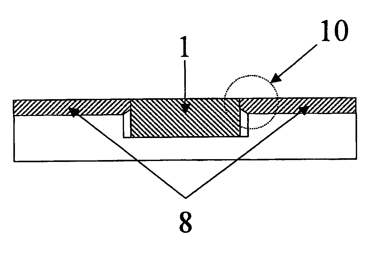
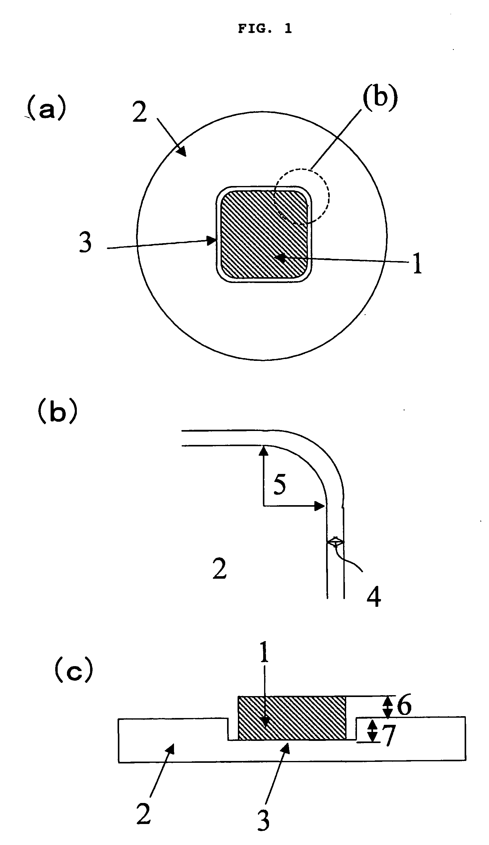
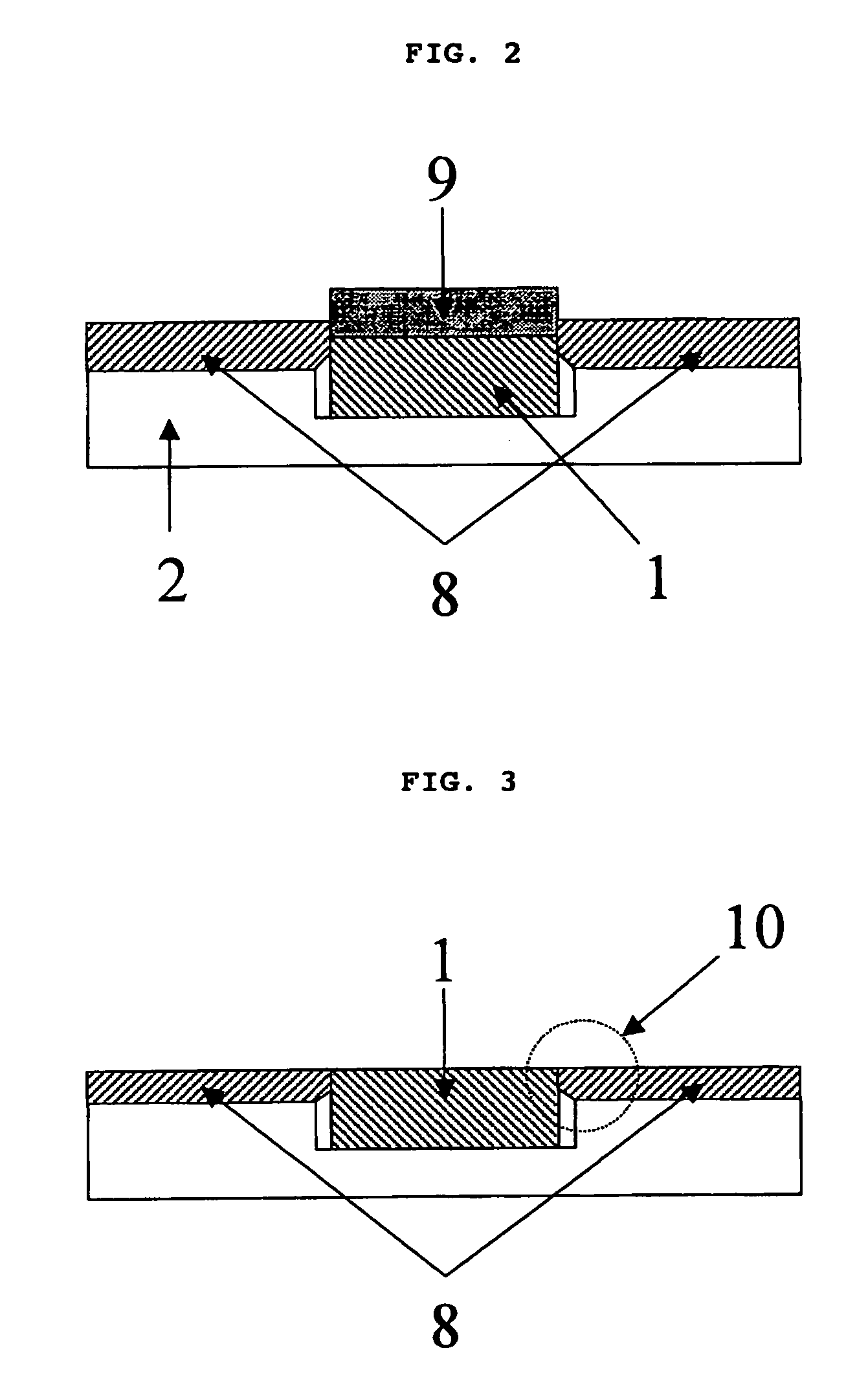
[0090]FIG. 7 is a schematic diagram of the mounting process. Three pieces of single crystalline diamond seed substrate were used. All were type IIa single crystalline diamond obtained by high-temperature high-pressure synthesis; the orientation of the main face was (111); and the size was a disk with a diameter of 2 mm, and a thickness of 100 μm. The main face of the silicon substrate 2 was (111) single crystalline substrate with a diameter of 2 inches and a thickness of 0.3 mm. As indicated in FIG. 7(a), three first regions 3 comprising concaves were formed on the main face of the silicon substrate by dry etching using a mask and high frequency plasma. The shape was cylindrical with a diameter of 2.05 mm and depth of 70 μm, and the side gap with respect to the single crystalline diamond seed substrate was 25 μm. As indicated in FIG. 7(b), after mounting the single crystalline diamond seed substrate, the stag...

example 3

[0102] In the present Example, the CVD diamond formation conditions during the were modified, then an example will be described of when the amount of warpage of the diamond substrate after connecting and polishing has been changed.

[0103] Seven samples were prepared in the same way as in the of Example 2.

[0104] The CVD diamond forming conditions were the same as those of the of Example 2 except for the temperature of the silicon substrate. The substrate temperature was varied in the range of 800 to 1100° C., and the warpage of the top surface (diamond surface) after formation of the various samples was set at −20 to +80 μm, and the warpage of the rear surface (silicon surface) was set at −20 to +20 μm. The thickness distribution of the diamond layer on the silicon substrate here was in the range of 5 to 90 μm respectively.

[0105] The same as that in Example 1 was conducted and the warpage of both surfaces after polishing were measured. Further, the photoresist coating described...


PUM

PropertyMeasurementUnit
corner radiiaaaaaaaaaa
corner angleaaaaaaaaaa
thicknessaaaaaaaaaa

Abstract

The present invention provides a manufacturing method for a large-scale diamond substrate and a substrate produced by the method suitable for semiconductor lithography processing and large-scale optical parts, semiconductor materials, thermal-release substrate, semiconductor wafer processing, and back-feed devices, and others. The manufacturing method for a diamond substrate of the present invention comprises: the mounting step of preparing a substrate having a main face comprising a first region which is a concave and having a second region which surrounds the first region, and mounting, on the first region, a single crystalline diamond seed substrate having a plate thickness thicker than the concave depth of the first region; a connecting step of forming a CVD diamond layer from the single crystalline diamond seed substrate using a chemical vapor deposition, and mutually connecting by forming a CVD diamond layer on the second region at the same time; and a polishing step of polishing to substantially flatten both the CVD diamond layers on the single crystalline diamond seed substrate and on the second region by mechanically polishing.

Description

TECHNICAL FILED [0001] The present invention relates to a substrate that includes a diamond single crystal and the manufacturing method thereof, and more particularly to a large-scale diamond substrate and manufacturing method thereof suitable for a semiconductor lithography process, large-scale optical parts, semiconductor materials and heat-release substrates and others. Further, the present invention relates to a large-scale conductive diamond substrate and manufacturing method thereof applicable to a semiconductor wafer process or the like, and applicable to the production of back-feed devices. BACKGROUND ART [0002] Diamond provides numerous superior characteristics such as high thermal conductivity, high electron / hole mobility, high dielectric breakdown field, low dielectric loss and wide band gap, and nothing else is similar as a semiconductor material. Specifically, electric field transistors with high frequency characteristics have recently been developed, and are expected t...

Claims


Application Information

Patent Timeline
Patent Type & Authority Applications(United States)
IPC IPC(8): C30B25/00
CPCC30B25/02C30B25/105C30B25/20C30B29/04H01L21/02381H01L21/0243H01L21/02527H01L21/0262H01L21/02645
Inventor MEGURO, KIICHITANIZAKI, KEISUKENAMBA, AKIHIKOYAMAMOTO, YOSHIYUKIIMAI, TAKAHIRO
Owner SUMITOMO ELECTRIC IND LTD
Why Eureka
Try Eureka