

Silicon wafer for IGBT and method for producing same
a technology of silicon wafers and silicon igbt, which is applied in the direction of silicon compounds, silicates, and under a protective fluid, can solve the problems of large influence of defects formed on the wafers, increase in production costs cannot be avoided, and the igbt is not easily destroyed, so as to prevent the generation of slip dislocations, prevent contamination of heavy metals, and resist high resistance
- Summary
- Abstract
- Description
- Claims
- Application Information
AI Technical Summary
Benefits of technology
Problems solved by technology
Method used
Image

Examples
examples
[0074] In the following, the present invention is explained in detail based on Examples. Example 1.
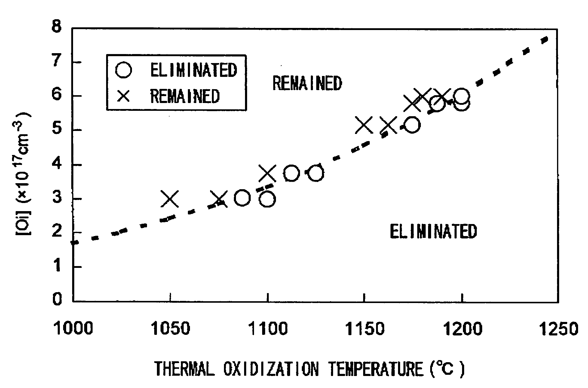
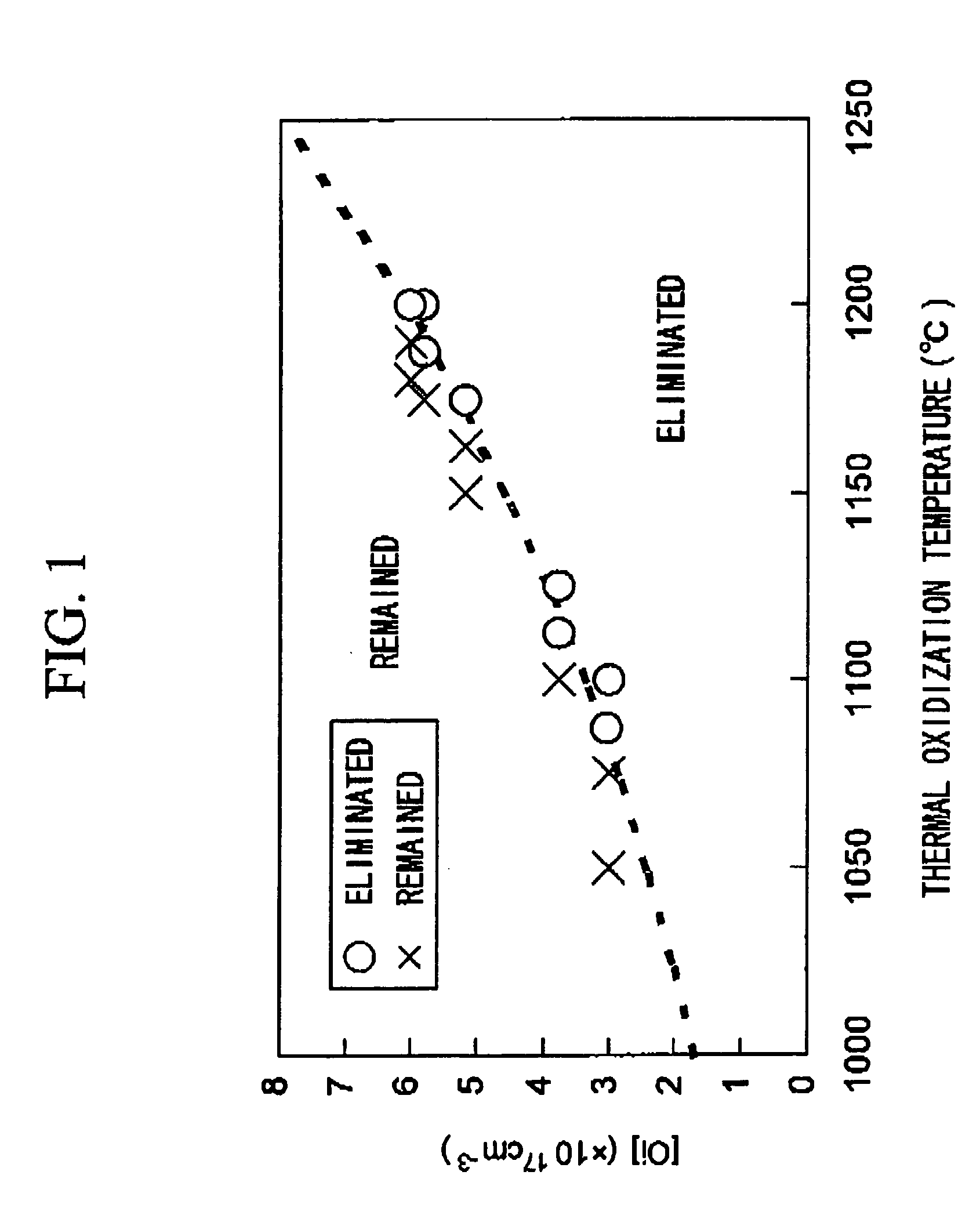
[0075] Firstly, silicon ingots of various interstitial oxygen concentrations were produced by the CZ method. Specifically, each single crystalline silicon ingot was prepared by the following steps. Firstly, a block of polycrystalline silicon was loaded in a quartz crucible, and a silicon melt was formed by heating the block of polycrystalline silicon in an Ar atmosphere. Next, a seed crystal was immersed in the silicon melt and was gradually pulled up while rotating the seed crystal and the crucible, thereby a single crystal was grown under the seed crystal. At that time, as an example of growth conditions, a ratio V / G of a growth rate V (mm / minute) of the crystal and thermal gradient G (° C. / mm) between the melting point and 1350° C. was controlled to be about 0.27. The interstitial silicon concentration was controlled by controlling rotation cycle of the quartz crucible and the pres...
example 2
[0084] Silicon ingots having various interstitial oxygen concentrations were produced by the CZ method. Those ingots were doped with nitrogen. Specifically, each single crystalline silicon ingot was prepared by the following steps. Firstly, a block of polycrystalline silicon was loaded in a quartz crucible, and a silicon melt was formed by heating the block of polycrystalline silicon in an Ar atmosphere. As a dopant of nitrogen, a silicon wafer having a nitride film was loaded to the silicon melt. Next, a seed crystal was immersed in the silicon melt and was gradually pulled up while rotating the seed crystal and the crucible, thereby a single crystal was grown under the seed crystal. At that time, the pulling rate of the crystal was controlled to be about 1.2 mm / minute. Thus, silicon ingots having an interstitial oxygen concentration of 3.5×10¹⁷ atoms / cm3 and nitrogen concentration of 2.5×10¹⁴ atoms / cm3 were produced.
[0085] COP density of the silicon ingots was measured to be 2.0×...
example 3
[0088] Silicon wafers of Example 3 of 200 mm in diameter were prepared by the same manner as Example 2 except that a silicon melt was not loaded with a silicon wafer having a nitride film. The silicon wafers of Example 3 had the same interstitial oxygen. concentration as that of the silicon wafers of Example 2.
Evaluation of Example 2 and Example 3.
[0089] COP densities of silicon wafers of Example 2 and Example 3 were measured by the same method and under the same conditions as those of Example 1. COP densities of the wafers of Example 2 and Example 3 were not more than 4.4×10⁴ / cm3. Therefore, it was confirmed that COPs were eliminated by the annealing in an oxidizing atmosphere.
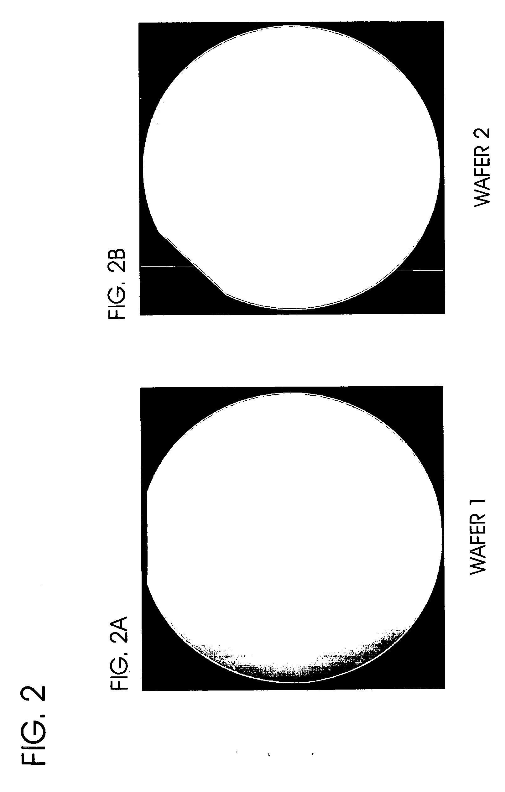
[0090] Next, the occurrence of slip dislocations in wafers of Example 2 and Example 3 were examined by X-ray topography. FIGS.3A to 3D show images of X-ray topography. As shown in FIGS. 3A to 3D, a slip dislocation was generated in lower right of the wafer of each example. In the nitrogen-doped wafers of E...
PUM
| Property | Measurement | Unit |
|---|---|---|
| thickness | aaaaa | aaaaa |
| size | aaaaa | aaaaa |
| diameter | aaaaa | aaaaa |
Abstract
Description
Claims
Application Information