Silicon Wafer Surface Defect Evaluation Method

a technology of silicon wafers and defects, applied in the direction of semiconductor/solid-state device testing/measurement, instruments, under protective fluids, etc., can solve the problems of increased leak current of devices, poor evaluation throughput, high cost, etc., and achieve the effect of detecting quickly a region

Active Publication Date: 2007-03-01
SUMCO CORP
View PDF21 Cites 7 Cited by
  • Summary
  • Abstract
  • Description
  • Claims
  • Application Information

AI Technical Summary

Benefits of technology

[0012] It is an object of the present invention to provide a silicon wafer surface defect evaluation method capable of readily detecting a region where a small crystal defect exists.
[0013] It is another object of the present invention to provide a silicon wafer surface defect evaluation method which facilitates manufacture of a silicon wafer formed of a defect-free region.
[0016] According to the present invention defined in claim 1, when a nitride film is generated on the wafer surface layer by applying the rapid heat treatment in the atmosphere which can nitride silicon under the above-described conditions, vacancies are injected into the wafer from the wafer surface. Defect in the region where the small COP's exist are coupled with the injected vacancies by heat simultaneously with the vacancy injection, and this coupling effectively acts as the center of re-coupling of the minority carrier As a result, in the region on the wafer surface where the small COP's which cannot be detected at least by the particle counter exist, a short diffusion length is detected. Calculating the minority carrier diffusion length on the wafer in this state by using the SPV method, since the COP's further effectively act as the center of re-coupling of the carrier, the region on the water surface where the small COP's which cannot be detected at least by the particle counter exist can be readily detected.
[0025] In the silicon wafer surface defect evaluation method according to the present invention, when a nitride film is generated on a wafer surface layer by applying a rapid heat treatment in an atmosphere which can nitride silicon under predetermined heating conditions, vacancies are injected into the wafer from the wafer surface. Defect existing in a region where small COP's exist are coupled with the injected vacancies by heat simultaneously with this vacancy injection, and this coupling effectively acts as a center of re-coupling of a minority carrier. As a result, in a region on the wafer surface where small COP's which cannot be detected at least by a particle counter exist, a short diffusion length is detected. When a minority carrier diffusion length on the wafer in this state is calculated by using the SPV method, since the COP's further effectively act as the center of re-coupling of the carrier, the region on the wafer surface in which the small COP's which cannot be detected at least by the particle counter exist can be readily detected. Moreover, since information such as a distribution with respect to crystal defects on the wafer can be accurately recognized, it is possible to conduct an examination to suppress generation of crystal defects from an initial stage of manufacture of the wafer based on such information, thereby facilitating production of the silicon wafer consisting of a defect-free region.

Problems solved by technology

Further, when the COP exists on a wafer surface, steps may be generated in a device wiring process, resulting in disconnection.
Furthermore, the COP can be a factor of leak or the like in an element isolation portion to lower a yield of a product.
This OISF causes a defect, e.g., an increase in a leak current of a device.
However, the evaluation method using the copper decoration method disclosed in Patent Reference 1 or Patent Reference 2 can detect a COP whose size is less than a detection lower limit of a particle counter, but it is complicated since many steps are required for measurement, and hence there has been a problem that an evaluation throughput is poor and a cost is high.

Method used


Image

  • Silicon Wafer Surface Defect Evaluation Method
  • Silicon Wafer Surface Defect Evaluation Method
  • Silicon Wafer Surface Defect Evaluation Method

Examples


example 1

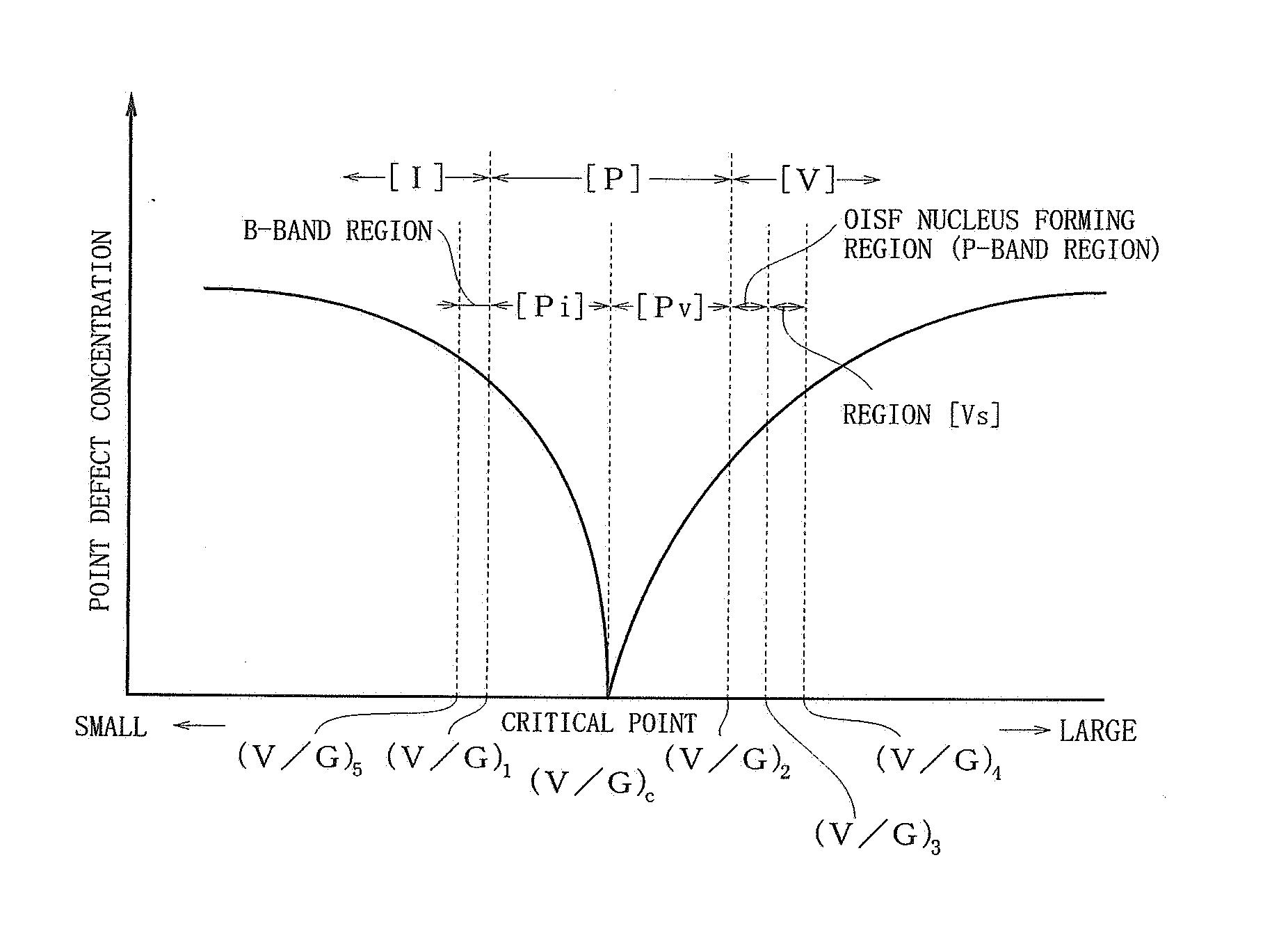
[0057] First, as shown in FIG. 1, a p-type silicon single-crystal ingot was pulled up, the ingot having a V / G ratio including a range of (V / G)1 to a critical point (V / G)c and a range of the critical point (V / G)c to (V / G)2, being controlled in such a manner that the V / C ratio consists of these ranges alone, and having a body portion with a diameter of 300 mm. This ingot was subjected to block cutting, external diameter grinding and orientation notch machining, and then it was sliced with a predetermined thickness, thereby a p-type silicon wafer having a diameter of 300 mm being cut out. A surface of this wafer was machine-polished to increase the parallelism, and thus an evaluation target wafer was provided.

[0058] Then, as a rapid heat treatment step, the wafer was put into a heat treatment furnace having an atmosphere which can nitride silicon by introducing a mixed gas containing an NH3 gas and an Ar gas at a ratio of 20:80, a heat treatment was performed at a temperature elevatin...

example 2

[0059] Surface defects on a wafer surface were detected like Example 1 except that a wafer cut out from a lot different from that of the wafer used in Example 1 was utilized as a measurement sample. That is, the wafer as an evaluation target in Example 2 is a wafer cut out from an ingot pulled up in a lot different from that of the ingot pulled up in Example 1. As shown in FIG. 1, like the ingot pulled up in Example 1, the ingot is a p-type silicon single-crystal ingot having a body portion with a diameter of 300 mm controlled in such a manner that a V / G ratio includes a range of (V / G)1 to a critical point (V / G)c and a range of the critical point (V / G)c to (V / G)2 and is composed of these ranges alone as pull-up conditions.

example 3

[0060] Surface defects on a wafer surface were detected like Example 1 except that a wafer cut out from a lot different from that of the wafers used in Examples 1 and 2 was utilized as a measurement sample. That is, the wafer as an evaluation target in this Example 3 is a wafer cut out from an ingot pulled up in a lot different from that of the ingots pulled up in Examples 1 and 2. Like the ingots pulled up in Examples 1 and 2, as shown in FIG. 1, the ingot is a p-type silicon single-crystal ingot having a body portion with a diameter of 300 mm controlled in such a manner that a V / G ratio includes a range of (V / G)1 to a critical point (V / G)c and a range of the critical point (V / G)c to (V / G)2 and is composed of these ranges alone as pull-up conditions of the ingot


PUM


Abstract

There is provided a silicon wafer surface defect evaluation method capable of readily detecting a region where small crystal defects exist. A silicon wafer surface defect evaluation method according to the present invention is characterized by comprising: a rapid heat treatment step of applying a heat treatment to a silicon wafer cut out from a silicon single-crystal ingot in an atmosphere which can nitride silicon at a temperature elevating speed of 10 to 150° C. / second from a room temperature to temperatures between not lower than 1170° C. and less than a silicon melting point, holding the silicon wafer at the processing temperature for 1 to 120 seconds and then cooling the silicon wafer to the room temperature at a temperature lowering speed of 10 to 100° C. / second; and a step of using a surface photo voltage method to calculate a minority carrier diffusion length on the wafer surface, thereby detecting a region on the wafer surface in which small COP's which cannot be detected at least by a particle counter exist.

Description

BACKGROUND OF THE INVENTION [0001] 1. Field of the Invention [0002] The present invention relates to a method of evaluating a surface defect of a silicon wafer cut out from a silicon single-crystal ingot (which will be referred to as an ingot hereinafter). More particularly, the present invention relates to a silicon wafer surface defect evaluation method which facilitates manufacture of a defect-free region silicon wafer cut out from an ingot grown by a Czochralski method (which will be referred to as a CZ method hereinafter). [0003] 2. Description of the Related Art [0004] With recent ultra-miniaturization of a semiconductor integrated circuit, as a factor which lowers a yield of a device, there is a crystal originated particle (which will be referred to as a COP hereinafter) which is a defect introduced in crystal growth, i.e., a defect formed in crystal growth of a silicon single-crystal ingot, a small defect of an oxygen precipitate which becomes a nucleus of an oxidation induc...

Claims


Application Information

Patent Timeline
IPC IPC(8): C30B15/00C30B21/06C30B27/02C30B28/10C30B30/04
CPCH01L22/12H01L22/00
Inventor ITOU, WATARUHASEGAWA, TAKESHISHIOTA, TAKAAKI
Owner SUMCO CORP
Why Eureka
Try Eureka