Thin film forming method

a thin film and formation method technology, applied in the direction of crystal growth process, monocrystalline material growth, semiconductor/solid-state device details, etc., can solve the problems of contamination particles, poor step coverage of pvd, non-even surface, etc., and achieve the effect of improving the purging

Inactive Publication Date: 2007-03-01
ASM KOREA LTD
View PDF41 Cites 15 Cited by
  • Summary
  • Abstract
  • Description
  • Claims
  • Application Information

AI Technical Summary

Benefits of technology

[0012] It is an object of the present invention to provide a method of for forming a metal layer, a metal oxide layer, or a metal nitride layer on a semiconductor or flat-panel display substrate with superior characteristics by chemical vapor deposition (CVD) in which a time-divisional sequentially-pulsed source supply technique is used along with plasma in synchronization with the sequentially pulsed source supply cycle.
[0013] In the present invention, a radio-frequency (RF) power of 0.01-2.0 W / cm2 is applied as pulses for plasma generation in synchronization with the cycle of pulsing reactant gases. Here, RF power means a maximum power level upon the application of power pulse. The plasma generation may be continuous rather than pulsed. When an atomic layer deposition (ALD) method using plasma is applied, the minimum reaction temperature at which source materials can be deposited into a layer is lowered. As a result, the range of reaction temperature at which a layer can be formed by ALD, from the maximum temperature to the minimum temperature, becomes broader. Therefore, although the ALD method is applied with many kinds of atoms to form a multi-atomic layer, an overlapping reaction temperature range between the atoms exists, thereby enabling formation of the multi-atomic layer by ALD. In other words, ALD using plasma (hereinafter, “plasma ALD”) is less limited in the range of minimum and maximum reaction temperatures, and thus selection of metallic source materials is also less limited, compared to a general ALD method not using plasma. In addition, when a pure metal layer is deposited using Al, Ti, or W, plasma serves as an activation energy source so that an atomic layer can be deposited at a temperature lower than the thermal decomposition temperature of the source material. The physical and chemical properties of the resultant layer can be varied and improved by changing the level of RF power pulses applied to generate plasma.
[0015] Here, to prevent unnecessary pre-reaction between source materials, the reactor is purged with a purge gas before and after each supply of source materials.
[0017] As a result, the deposition rate of the metal oxide layer is improved, compared to the method using a purge gas. As another example, a metal nitride layer can be formed using nitrogen gas (N2) and hydrogen gas (H2) which do not react with a metallic source, by pulsing materials in the following sequence: [(metallic source)→(nitrogen gas+hydrogen gas)→(nitrogen and hydrogen plasma)→].
[0019] According to the present invention, oxygen gas, hydrogen gas, and a mixture of nitrogen and hydrogen can be mixed with an inert gas such as helium (He) or argon (Ar) to be used as a purge gas for improved purging effects. The addition of an inert gas also allows reactivity to be controlled by varying the concentration of reactant gas.

Problems solved by technology

However, PVD is known to have poor step coverage and produce a non-even surface due to an overhang phenomenon where the opening of a hole or a trench is closed before the hole or trench are fully filled.
However, for the conventional CVD technique, the source materials required to form a layer are supplied at the same time, and therefore it is difficult to form a target layer having a desired composition and property.
In addition, reaction of a variety of materials used to form a layer occurs in the gas phase, thereby causing the generation of contamination particles.
As a result, it becomes difficult to form a layer having a uniform composition over a large area on the surface of a 300-mm wafer.
Therefore, when a multicomponent metal oxide film is formed by ALD, the thin film formation process become complicated, and a complex manufacturing apparatus is required.
However, simultaneous supply of the precursors containing the respective constituent metal atoms in this method causes reaction between the constituent metal atoms, thereby lowering the vapor pressure.
Once particles are generated, removing as well as handling of such particles is very difficult.
Ba(thd)2 and Sr(thd)2, which are Ba and Sr precursors, respectively, react with an alkyl group precursor to form a compound having a low vapor pressure, which is difficult to handle.
Furthermore, if the temperature of the substrate is too low, the target layer cannot be formed because a desired reaction does not occur between supplied source gases.
If a target layer is composed of many kinds of atoms so that there is no overlapping range of reaction temperatures between the constituent atoms, ALD methods cannot be applied to form the target layer.
In addition, it is impossible to deposit a pure metal layer such as a Ti, W, or Al layer at a temperature lower than the thermal decomposition temperature of the metal layer by conventional ALD methods.
Thus, it takes a considerable amount of time to fully exhaust the remaining reactant gas from the reactor.
When plasma is directly generated in a reactor for a faster reaction rate, the method by Sherman et al. causes a serious change in gas pressure of the reactor, thereby destabilizing plasma.
In this case, the method by Sherman et al. leads to clogging of the liquid source supply unit.
As a result, a viscous solid material remains in the liquid source supply unit and clogs the supply line of the liquid source.

Method used


Image

  • Thin film forming method
  • Thin film forming method
  • Thin film forming method

Examples


embodiment 1

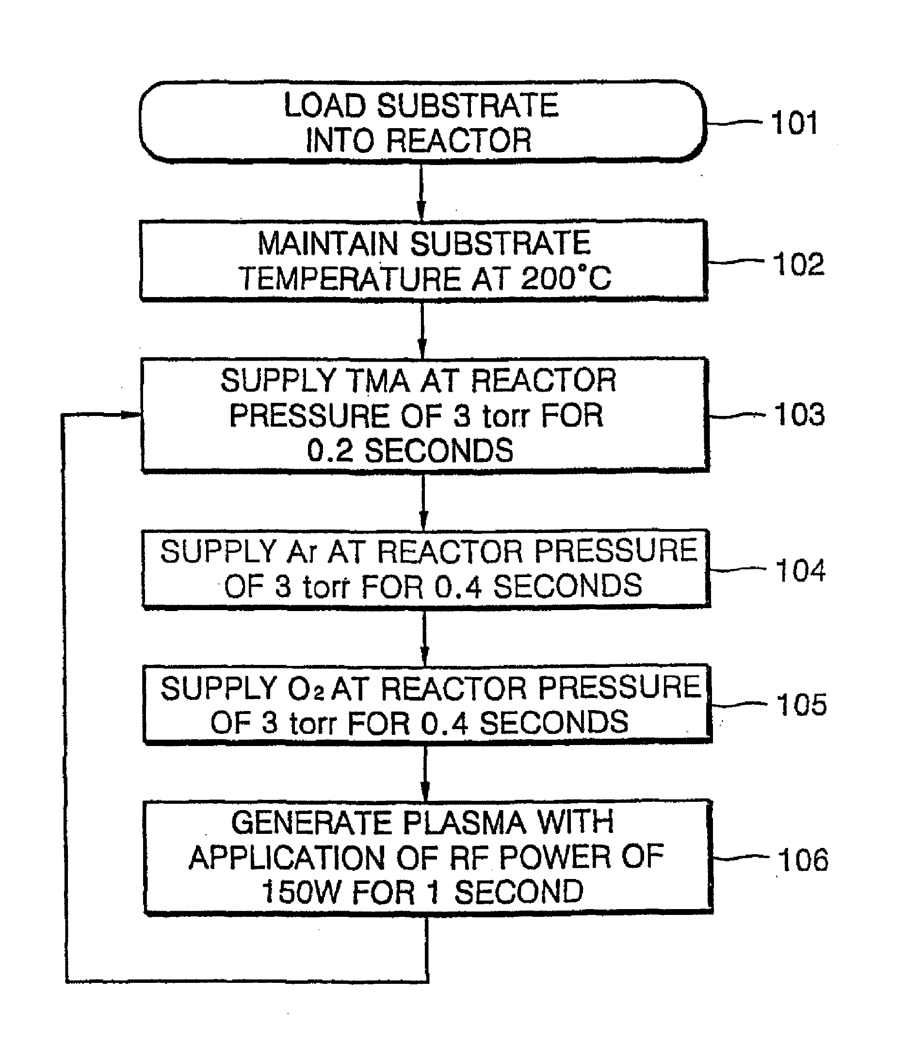
[0026] Oxygen gas (O2) reacts slowly with an organometallic source material so that it is difficult to form a metal oxide layer at a temperature of 400° C. or less with oxygen gas and an organometallic source material. Although a metal oxide layer can be formed with oxygen gas and an organometallic source material, the film formation rate is very slow. Thus, in the present embodiment, a method of forming an aluminum oxide layer using oxygen plasma is described. FIG. 1 is a flowchart illustrating an ALD method according to a first embodiment of the present invention.

[0027] As shown in FIG. 1, an aluminum oxide (Al2O3) layer was formed using trimethylaluminum (TMA) as an aluminum source at a substrate temperature of 200° C. at a reactor pressure of 3 torr. To form the aluminum oxide layer, TMA is supplied for 0.2 seconds, argon (Ar) for 0.4 seconds, and oxygen gas (O2) for 0.4 seconds in sequence, and directly followed by oxygen plasma generation for 1 second (Step 103 through 106 of...

embodiment 2

[0030]FIG. 3 is a flowchart illustrating a second embodiment of an ALD method for forming a tantalum oxide (Ta2O5) layer according to the present invention. As shown in FIG. 3, a tantalum oxide (Ta2O5) layer was formed using dimethoxyamidoethyltetraethyltantalum (Ta(OC2H5)4(OCH2(CH2N(CH3)2), TAE(dmae)) as a tantalum source at a substrate temperature of 250° C. at a reactor pressure of 4 torr. To form the tantalum oxide layer, the sequential processing step of TAE(dmae) (0.3 sec)→Ar(1.7 sec)→O2 (1 sec)→(O2+plasma) (2 sec)→Ar(1 sec) is followed, during which cycle a plasma is generated for 2 seconds with oxygen (O2) gas. The sequential pulses of gases and plasma generation totaling 6 seconds are referred to as a cycle (Step 303 through 307 of FIG. 3). Here, a radio frequency (RF) power of 180 W is applied for 2 seconds in order to generate oxygen plasma. The completion of one cycle resulted in a tantalum oxide layer having a thickness of 0.67 Å.

[0031] A conventional ALD method, which...

embodiment 3

[0033] The present embodiment is directed to a plasma ALD method for forming a strontium titanate (SrTiO3; STO) layer. STO or barium strontium titanate ((Ba,Sr)TiO3; BST) has greater dielectric constant so that they are used as a dielectric material for capacitors of highly integrated memory devices such as DRAMs.

[0034] A source material Sr(thd)2, where abbreviation “thd” stands for tetramethylheptanedionate, is supplied into a reactor and then the reactor is purged with argon (Ar). Next, oxygen gas is supplied into the reactor to generate plasma and then the reactor is purged again with Ar. Ti(O-i-Pr)4 [or Ti(O-i-Pr)2(thd)2] is supplied into the reactor, and the reactor is purged again with Ar gas. Next, oxygen gas is supplied into the reactor to generate plasma and then the reactor is purged with Ar. This cycle is repeated one or more times until a STO layer having a desired thickness is obtained.


PUM

PropertyMeasurementUnit
pressureaaaaaaaaaa
temperatureaaaaaaaaaa

Abstract

A method for forming thin films of a semiconductor device is provided. The thin film formation method presented here is based upon a time-divisional process gas supply in a chemical vapor deposition (CVD) method, where the process gases are supplied and purged sequentially, and additionally plasma is generated in synchronization with the cycle of pulsing reactant gases. A method of forming thin films that possess a property of gradient composition profile is also presented.

Description

CROSS-REFERENCE TO RELATED APPLICATIONS [0001] This application is a continuation of U.S. patent application Ser. No. 10 / 297,867, filed Jul. 15, 2003, entitled “THIN FILM FORMING METHOD,” which is the national phase application of PCT / KR01 / 00974, filed Jun. 8, 2001, and claims priority from Korean Application No. 2000-31367 filed Jun. 8, 2000; and Korean Application No. 2001-3830 filed Jan. 26, 2001, which are incorporated herein by reference.BACKGROUND OF THE INVENTION [0002] 1. Field of the Invention [0003] The present invention relates to a thin film formation method, and more particularly, to a method for forming a metal film, a metal oxide film or a metal nitride film that can be used as an insulating layer, a dielectric layer, or an interconnect layer in a semiconductor or flat-panel display substrate. [0004] 2. Description of the Related Art [0005] In the prior art, a metal film, a metal oxide film, or a metal nitride film have been formed by means of a physical vapor deposit...

Claims


Application Information

Patent Timeline
Patent Type & Authority Applications(United States)
IPC IPC(8): C23C16/00H05H1/24C23C16/34C23C16/36C23C16/18C23C16/40C23C16/44C23C16/455C23C16/50C23C16/515H01L21/283H01L21/285H01L21/314H01L21/316H01L21/3205H01L21/768H01L23/522
CPCC23C16/34C23C16/36C23C16/40C23C16/403H01L21/31691C23C16/409C23C16/4554C23C16/515C23C16/405H01L21/02274H01L21/02148H01L21/02183H01L21/02178H01L21/0228H01L21/02159H01L21/02197
Inventor KOH, WON-YONGLEE, CHUN-SOO
Owner ASM KOREA LTD
Why Eureka
Try Eureka