Anisotropic etching method

a etching method and anisotropic technology, applied in the field of anisotropic etching method, can solve the problems of etching more anisotropic without increasing the duration of the etching operation, and the cost of a very slow rate of attack, etc., to achieve the effect of strengthening or, less sensitive to the variation of process parameters, easy sublimation

Inactive Publication Date: 2007-08-23
TEGAL CORP
View PDF11 Cites 10 Cited by
  • Summary
  • Abstract
  • Description
  • Claims
  • Application Information

AI Technical Summary

Benefits of technology

[0039] The method of the invention aims to strengthen or to ensure the integrity of the passivating layer that protects the etched flanks throughout the etching step in order to make it less sensitive to variations in the process parameters. In fact this layer is very fragile and in particular gives rise to irreversible defects produced during etching by the prior art methods. The passivating layer produced by the method according to the present invention has the particular feature of sublimating easily when the temperature rises above −70° C. By avoiding the presence of the C, CxFy or PTFE type pollutants of the prior art methods, the passivating layer gives the method the advantage of being a very clean etching method. The walls of the chambers remain clean and the surfaces of the substrates are therefore always clean. This is an important advantage from the industrial point of view because the steps of cleaning these chambers, mechanically or by means of a plasma, are no longer necessary. This increases the a

Problems solved by technology

Gases based on halogens other than fluorine, such as chlorine, bromine or iodine, enable anisotropic etching of silicon, but at the cost of a very slow rate of attack, and so are rarely used in practice.
The problem is therefore to make etching more anisotropic without increasing the duration of the etching operation.
This technique has a number of drawbacks, however, such as that of being “dirty” and highly sensitive to the condition of the walls of the reactor.
On the one hand, the time necessary to remove the film in the bottom of the trench induces a process time that is not used to attack the silicon, which entails an increase in the overall duration of the step of etching the substrate.
On the other hand, the use of a fluorocarbon gas such as C4F8 is costly.
Moreover, this method is highly sensitive to the state of the walls of the processing chamber.
The pollution resulting from the presence of a gas forming a polymer necessitates a cleaning operation after the etching operation, which slows do

Method used


Image

  • Anisotropic etching method
  • Anisotropic etching method
  • Anisotropic etching method

Examples


Embodiment Construction

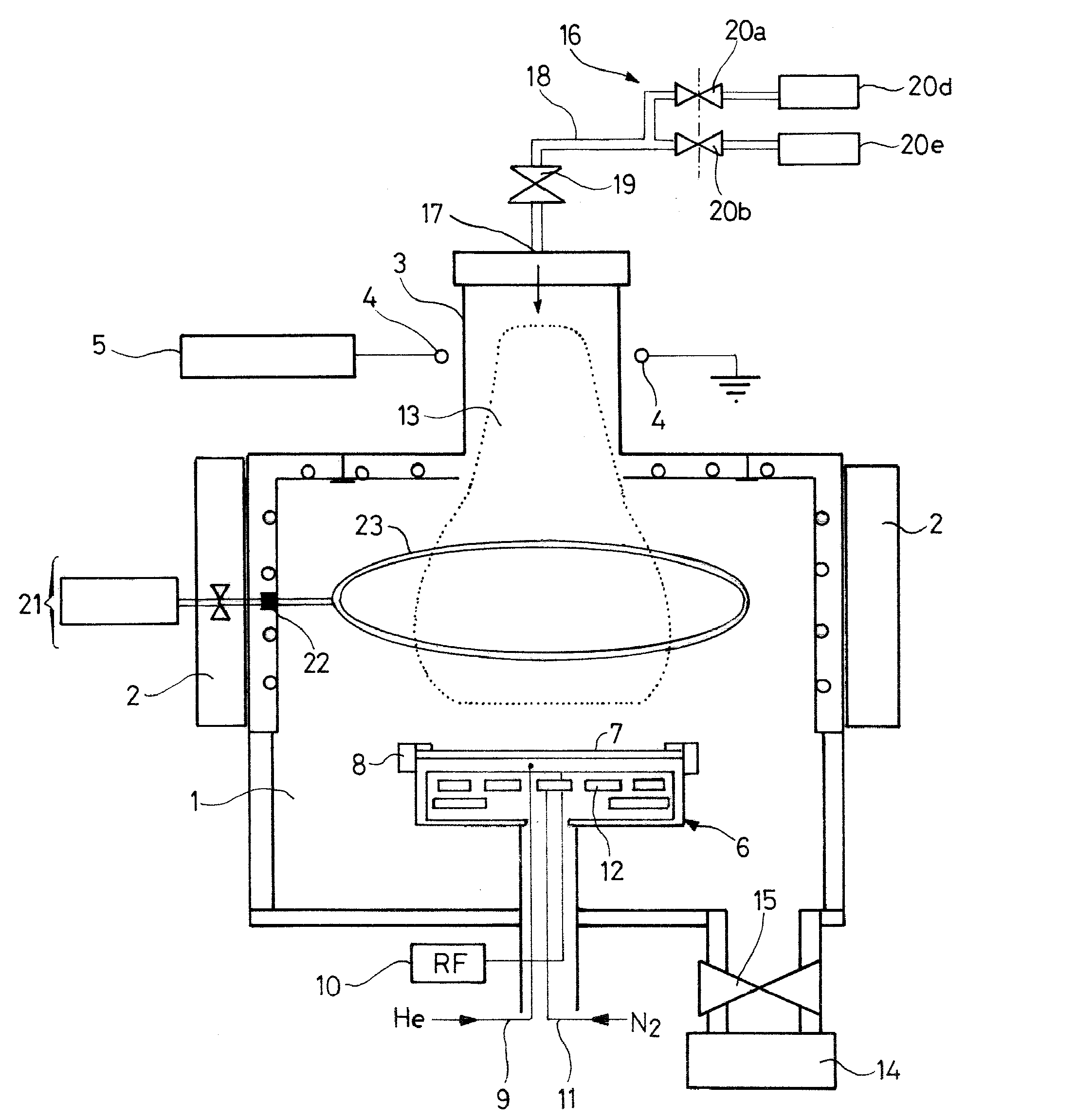
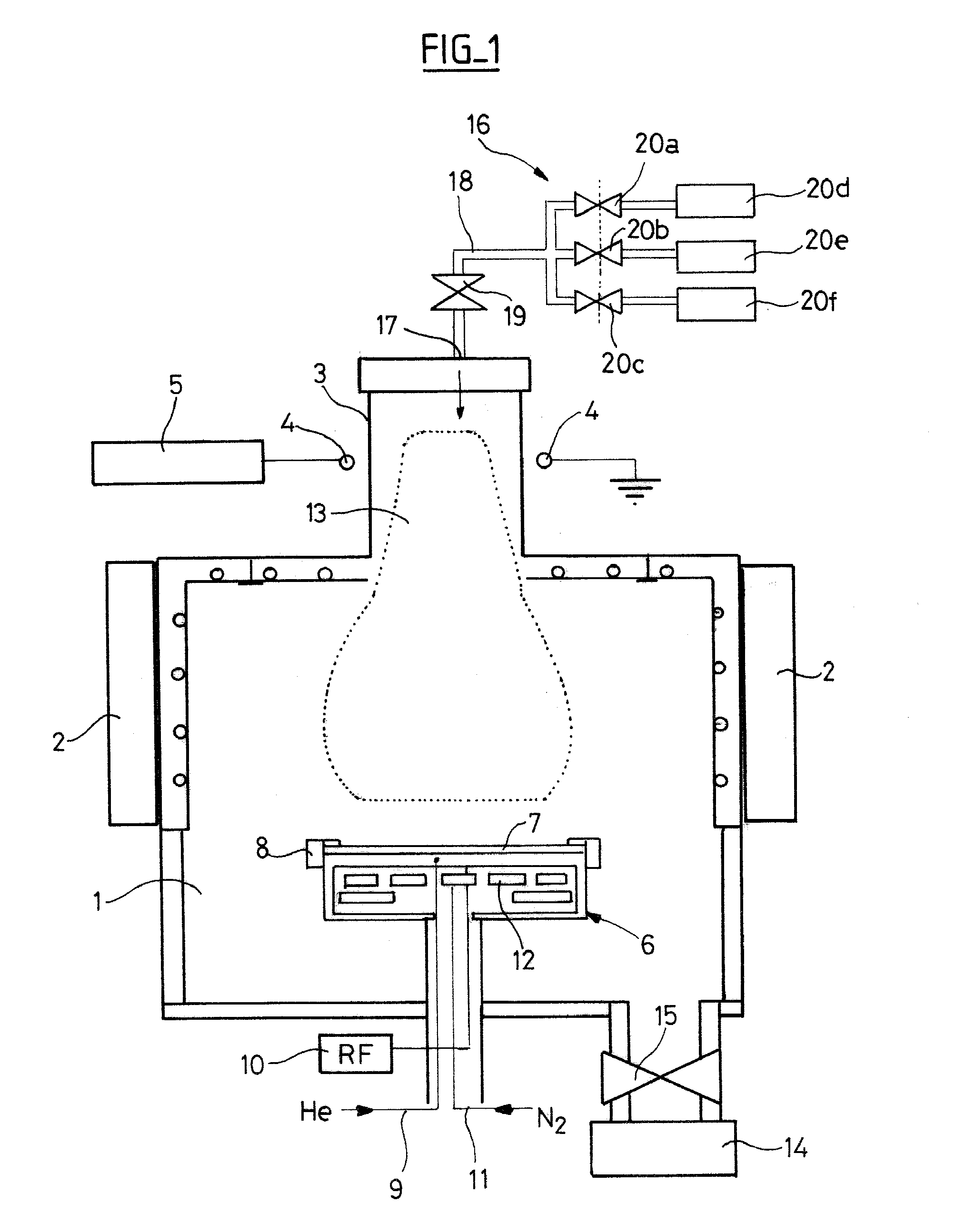
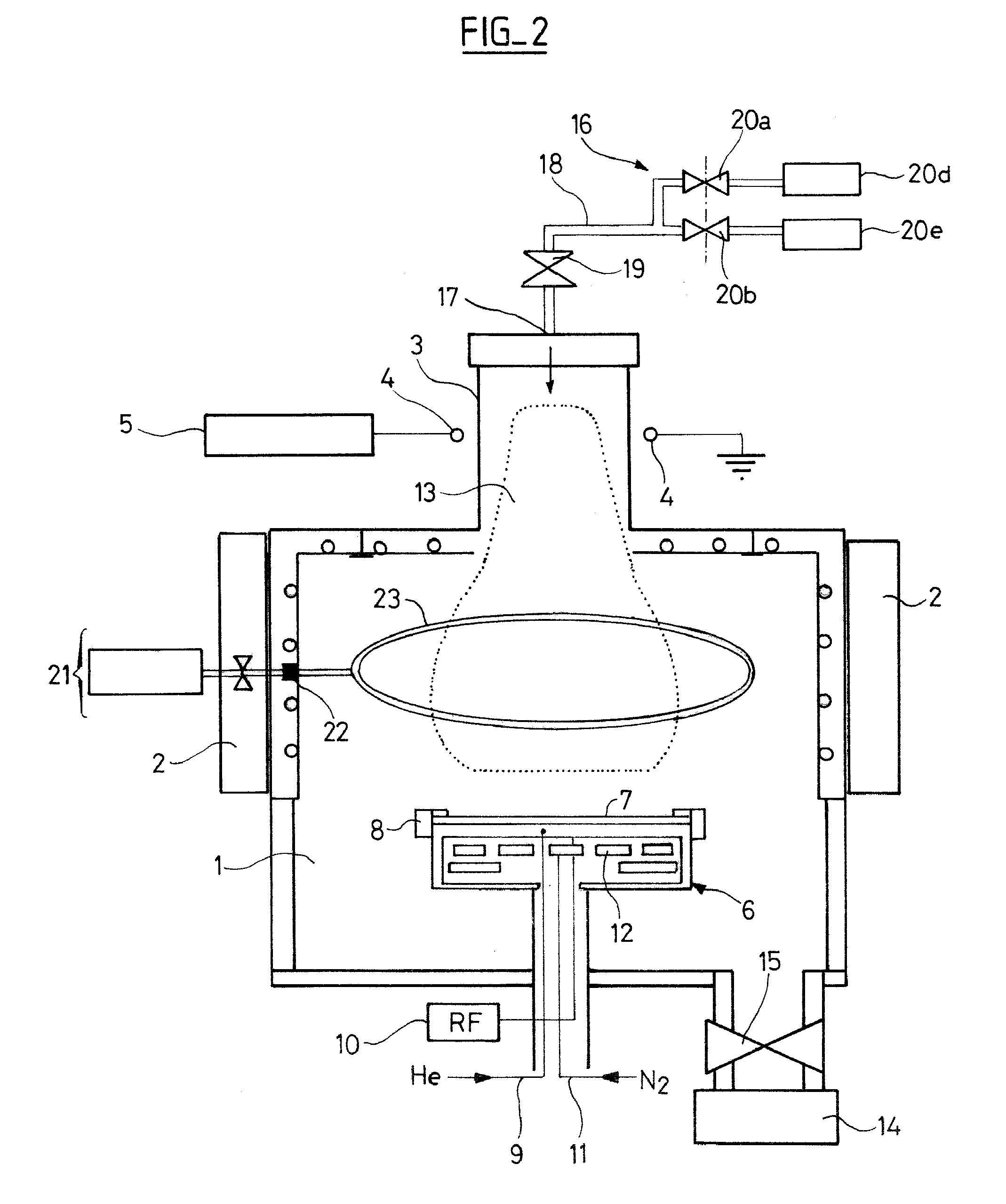
[0045] The device represented in FIG. 1 is a plasma etching machine that comprises a process chamber 1 surrounded by permanent magnets 2 in a multipolar arrangement to reduce electron loss at the walls of the chamber. The chamber 1 communicates with a plasma source the dielectric material tube 3 whereof, in which the plasma is formed, is surrounded by a coupling electrode 4 fed with radio-frequency (RF) alternating current by an RF generator 5 supplying an RF (13.56 MHz) power P from 500 W to 2000 W.

[0046] The chamber 1 contains a substrate-carrier 6. A substrate 7 to be etched approximately 100 mm thick is fixed to the substrate-carrier 6 by mechanical or electrostatic means, here mechanically by means of a ring 8, for example. The substrate 7 is separated from the substrate-carrier 6 by a film 9 of helium. A bias voltage U from 20 V to 60 V, preferably of the order of 50 V, is applied to the substrate 7 by means of an RF (13.56 MHz) or low-frequency (50-500 kHz) generator 10. The...


PUM

PropertyMeasurementUnit
Temperatureaaaaaaaaaa

Abstract

The present invention consists in a method for anisotropically etching a silicon substrate at very low temperature using a high-density fluorinated gas plasma, characterized in that the plasma is formed from a gas mixture comprising an etching gas containing fluorine, a passivating gas containing oxygen and a reaction gas comprising chlorine, and in which method the respective ratios of the flowrate of the passivating gas and the flowrate of the reaction gas to the flowrate of the etching gas are less than 0.15 by volume. The etching gas containing fluorine is preferably sulfur hexafluoride SF6, the passivating gas containing oxygen is preferably chosen from oxygen O2, ozone O3 and sulfur dioxide SO2, and the reaction gas comprising chlorine is preferably silicon tetrachloride SiCl4.

Description

CROSS-REFERENCE TO RELATED APPLICATIONS [0001] This application is based on French Patent Application No. 0650357 filed Feb. 1, 2006, the disclosure of which is hereby incorporated by reference thereto in its entirety, and the priority of which is hereby claimed under 35 U.S.C. §119. BACKGROUND OF THE INVENTION [0002] 1. Field of the Invention [0003] The present invention relates to a method of etching anisotropically at very low temperature using a high-density fluorinated gas plasma to produce microreliefs on the surface of semiconductor substrates, in particular silicon substrates for the production of semiconductor components and microsystems known as micro-electro-mechanical systems (MEMS) and micro-opto-electro-mechanical systems (MOEMS). [0004] 2. Description of the Prior Art [0005] These Microsystems necessitate deep and highly anisotropic etching with high selectivity and high rates of attack. Techniques based on non-toxic, non-corrosive and simple chemistries are preferabl...

Claims


Application Information

Patent Timeline
IPC IPC(8): H01L21/306C23F1/00
CPCH01J37/321H01L21/3065H01J2237/2001
Inventor PUECH, MICHEL
Owner TEGAL CORP
Why Eureka
Try Eureka