Structures and methods for low-k or ultra low-k interlayer dielectric pattern transfer

a dielectric pattern and interlayer technology, applied in the field of structures and methods for low-k or ultra-low-k interlayer dielectric pattern transfer, can solve the problems of non-scalable factors in interconnect scaling that add to the thickness, undesirable collapse of the resist layer, and overall dimension reduction impose significant limitations on the dimensions so as to increase the width of the resist pattern, and reduce the cds or line width

Inactive Publication Date: 2007-11-08
GLOBALFOUNDRIES INC
View PDF12 Cites 9 Cited by
  • Summary
  • Abstract
  • Description
  • Claims
  • Application Information

AI Technical Summary

Benefits of technology

[0018] The present invention provides a novel approach to fine pitch wiring pattern transfer. The initial critical dimensions (CDs) or line widths, as defined by the initial lithographic pattern, is provided in the present invention at about 10-15 nm smaller than the targeted CDs or line widths. The reduced CDs or line widths lead to increase in the line spacing, as well as increase in the widths of the resist pattern. Correspondingly, the thickness of the resist pattern can be increased significantly (e.g., for about 40%), without increasing the aspect ratio thereof. In other words, the vertical budget of the resist pattern is increased without increasing the r

Problems solved by technology

Higher aspect ratio for the resist pattern is desirable for subsequent pattern transfer, i.e., a thicker resist layer provides more protection for the masked regions in the underlying layers, but it can lead to undesirable collapse in the resist layer during the image developing process.
The hard mask layer is employed during the pattern transfer process because the organic resist material is not suitable for direct image transfer into the ILD layer by RIE.
The overall dimension reduction imposes significant limitations on the dimensions of the resist patterns.
However, there are several non-scalable factors in the interconnect scaling that add to the thicknesses of the underlying dielectric layer(s).
Such non-scalable factors as illustrated hereinabove significantly limit possible reduction in the depth of the underlying dielectric layers.
Such limitations, which are placed on the resist pattern thickness by the overall semiconductor dimension scaling on one hand and by the non-scalable factors in the dielectric depth on the other hand, in turn limit the possible choices of the hard mask structures that can be used for pattern transfer from the resist layer to the underly

Method used


Image

  • Structures and methods for low-k or ultra low-k interlayer dielectric pattern transfer
  • Structures and methods for low-k or ultra low-k interlayer dielectric pattern transfer
  • Structures and methods for low-k or ultra low-k interlayer dielectric pattern transfer

Examples


Embodiment Construction

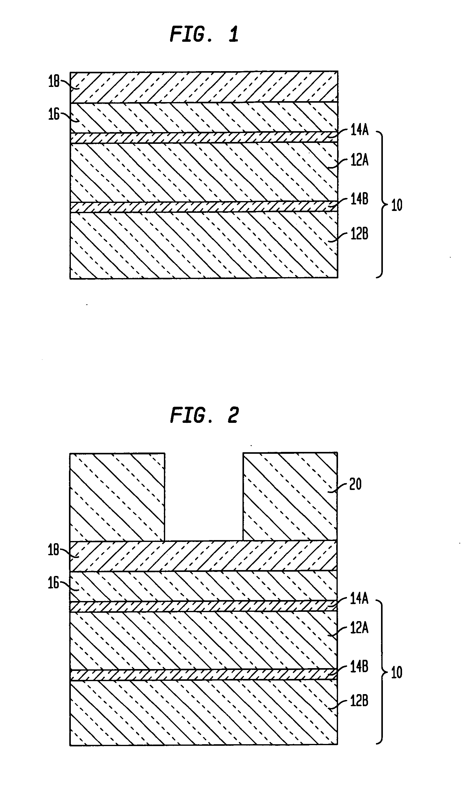
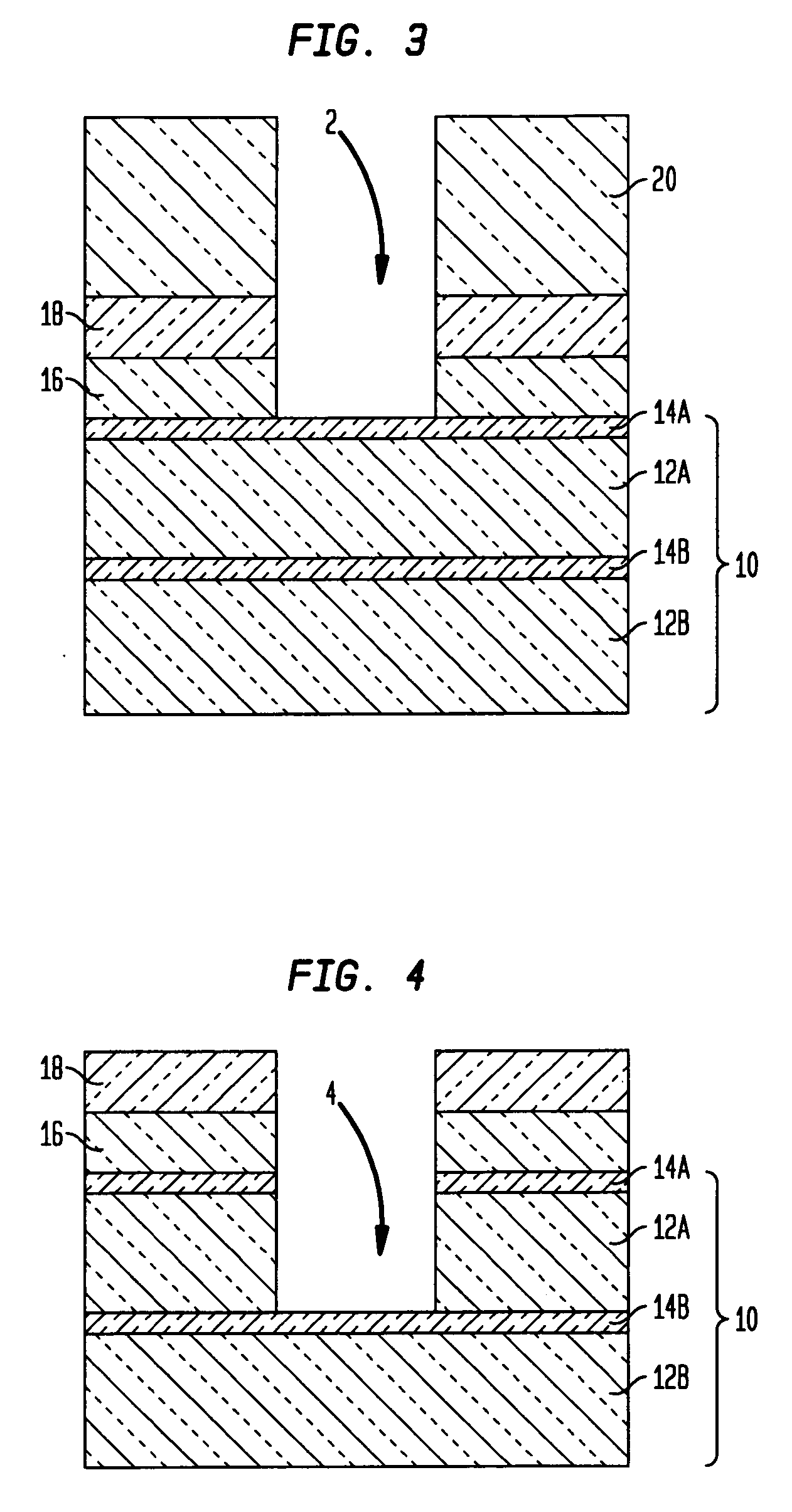
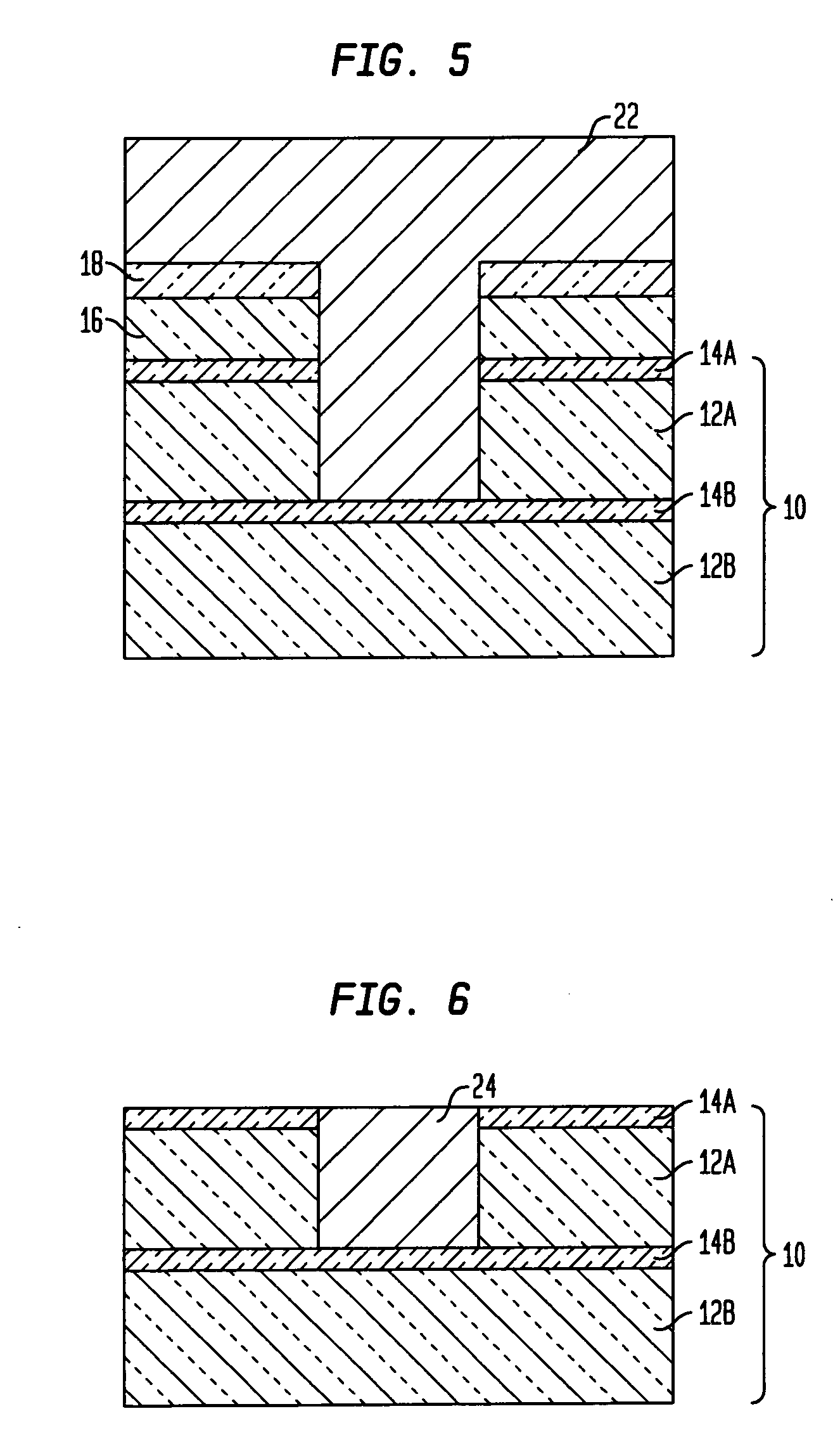
[0043] In the following description, numerous specific details are set forth, such as particular structures, components, materials, dimensions, processing steps and techniques, in order to provide a thorough understanding of the present invention. However, it will be appreciated by one of ordinary skill in the art that the invention may be practiced without these specific details. In other instances, well-known structures or processing steps have not been described in detail in order to avoid obscuring the invention.

[0044] It will be understood that when an element as a layer, region or substrate is referred to as being “on” or “over” another element, it can be directly on the other element or intervening elements may also be present. In contrast, when an element is referred to as being “directly on” or “directly over” another element, there are no intervening elements present. It will also be understood that when an element is referred to as being “beneath” or “under” another elem...


PUM

PropertyMeasurementUnit
Thicknessaaaaaaaaaa
Thicknessaaaaaaaaaa
Nanoscale particle sizeaaaaaaaaaa

Abstract

The present invention relates to improved methods and structures for forming interconnect patterns in low-k or ultra low-k (i.e., having a dielectric constant ranging from about 1.5 to about 3.5) interlevel dielectric (ILD) materials. Specifically, reduced lithographic critical dimensions (CDs) (i.e., in comparison with target CDs) are initially used for forming a patterned resist layer with an increased thickness, which in turn allows use of a simple hard mask stack comprising a lower nitride mask layer and an upper oxide mask layer for subsequent pattern transfer. The hard mask stack is next patterned by a first reactive ion etching (RIE) process using an oxygen-containing chemistry to form hard mask openings with restored CDs that are substantially the same as the target CDs. The ILD materials are then patterned by a second RIE process using a nitrogen-containing chemistry to form the interconnect pattern with the target CDs.

Description

FIELD OF THE INVENTION [0001] The present invention generally relates to interconnect pattern formation in the sub-60 nm generations of semiconductor devices as addressed by the International Technology Roadmap for Semiconductor (ITRS), including the 45 nm node, the 33 nm node, and the 22 nm node devices. More specifically, the present invention relates to lithographic resist patterning and transfer of the resist pattern to a hard mask stack and then to a low-k (i.e., having a dielectric constant k ranging from about 2.2 to about 3.5) or ultra low-k (i.e., having a dielectric constant k below 2.4) interlevel dielectric structure for formation of at least one interconnect pattern within the dimensions mentioned hereinabove. BACKGROUND OF THE INVENTION [0002] In a conventional interconnect pattern formation process, a hard mask layer is first formed over the ILD layer in which an interconnect pattern is to be formed, and a photo- or electron beam-sensitive resist layer is then coated ...

Claims


Application Information

Patent Timeline
IPC IPC(8): G03F7/26
CPCH01L21/31144H01L21/76813H01L21/76802
Inventor BUCCHIGNANO, JAMES J.GIBSON, GERALD W.ROTHWELL, MARY B.YU, ROY R.
Owner GLOBALFOUNDRIES INC
Why Eureka
Try Eureka