Surface Modification Method for Solid Sample, Impurity Activation Method, and Method for Manufacturing Semiconductor Device

Inactive Publication Date: 2007-12-20
ELECTRO-MOTIVE DIESEL
View PDF2 Cites 24 Cited by
  • Summary
  • Abstract
  • Description
  • Claims
  • Application Information

AI Technical Summary

Benefits of technology

[0077] To solve the above problems, the surface modification method for a solid sample according to the present invention includes a step of irradiating the solid sample with a pulsed laser light having a pulse width within the range from 10 to 1000 femtoseconds so as to modify only the surface layer of the solid sample from a crystalline phase to an amorphous phase or from an amorphous phase to a crystalline phase. Since the ion implantation process is not performed, the modified layer formed on the solid sample can have a uniform

Problems solved by technology

The miniaturization of the MOS transistors inevitably causes the short channel effect.
The decrease in the junction depth of the source/drain extension regions also causes an increase in the parasitic resistance, which makes it more difficult to increase the device speed.
This means that it is necessary to create a junction that is ultra-shallow and yet has a very low resistance.
This requirement is difficult to satisfy.
Whether or not these tech

Method used


Image

  • Surface Modification Method for Solid Sample, Impurity Activation Method, and Method for Manufacturing Semiconductor Device
  • Surface Modification Method for Solid Sample, Impurity Activation Method, and Method for Manufacturing Semiconductor Device
  • Surface Modification Method for Solid Sample, Impurity Activation Method, and Method for Manufacturing Semiconductor Device

Examples


Example

Embodiment 1

[0124] This section describes an embodiment of the present invention on the basis of FIGS. 2 to 6.

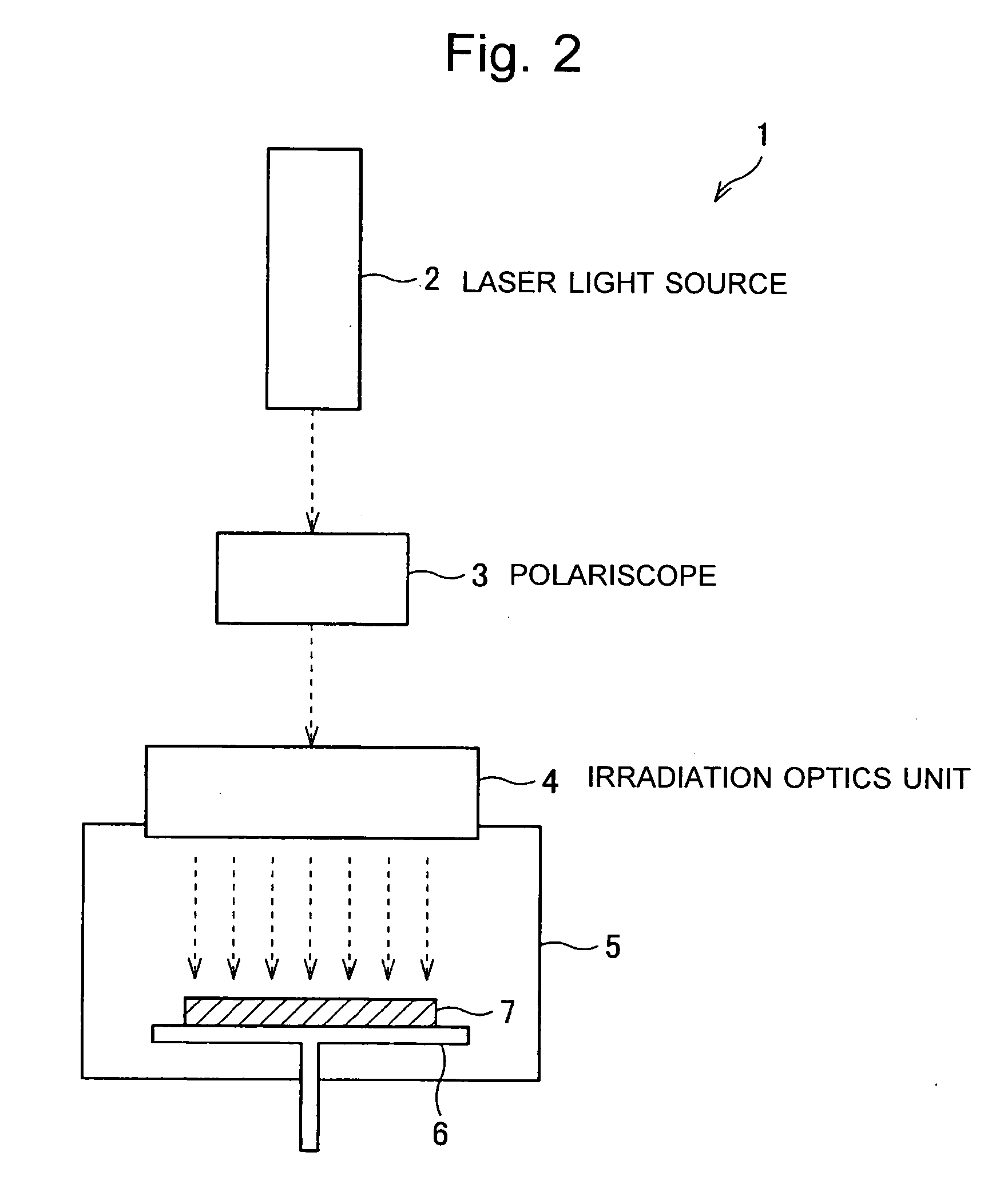
[0125]FIG. 2 is a schematic diagram showing an ultra-short pulsed laser irradiation system 1 of the present embodiment. As shown in FIG. 2, the irradiation system 1 includes a laser light source 2, a polariscope 3, an irradiation optics unit 4 and a chamber 5.

[0126] The laser light source 2 generates an ultra-short pulsed laser light having a pulse width within a range from 10 to 1000 femtoseconds, which corresponds to a frequency band from 1 to 100 THz. An example is a titanium-sapphire laser. The laser light source 2 can control the pulse width, the laser fluence, the number of pulse shots and the wavelength of the laser light to be produced. The laser fluence hereby means the density of radiation energy. The laser fluence is controlled through the output energy and the spot diameter of the laser light generated by the laser light source 2.

[0127] The polariscope 3, whi...

Example

Example 1-2

[0135] As opposed to Example 1-1, the present example is an example in which an amorphous phase was modified to a crystalline phase. As in the previous example, a titanium-sapphire laser was used as the laser light source 2. A single-crystal silicon substrate, on which an amorphous layer of about 10 nm in thickness was formed by implanting germanium ions by 5 keV, was used as the solid sample 7.

[0136]FIG. 6 shows the lattice images of the surface region of the single-crystal silicon substrate with the amorphous layer formed on it. The images were taken with a TEM before and after the irradiation of the ultra-short pulse laser light, respectively. FIG. 6(b) is an enlarged image of FIG. (a).

[0137] As shown in FIG. 6, it was confirmed that the amorphous layer formed from the surface to a depth of 10 nm was changed to a crystalline phase by an irradiation of an ultra-short pulsed laser light. This proves that an amorphous phase can be changed to a crystalline phase by an i...

Example

Embodiment 2

[0155] In the previous embodiment, the solid sample 7 was irradiated with an ultra-short pulsed laser light to excite the surface of the solid sample 7 before the modification of the surface (e.g. modification from a crystalline phase to an amorphous phase) or activation of the impurity layer 16. In general, excitation of a surface can be done by increasing the laser fluence. However, as described previously, this operation is undesirable because it causes ablation. The present embodiment provides a method for further helping the surface excitation of the solid sample 7 while suppressing the ablation.

[0156] In the present embodiment, the solid sample 7 made of a semiconductor material is irradiated with an electromagnetic wave to excite the valence electrons to the conduction band before the irradiation of the ultra-short pulsed laser light. Examples of the excitation methods include a multi-photon process; in a preferable method, the solid sample 7 is irradiated with ...


PUM


Abstract

The present invention intends to provide a method for manufacturing a semiconductor device in which source/drain extension regions having a uniform depth are created with high reproducibility. This objective is achieved by the following method: A gate electrode 24 is formed on a semiconductor substrate 21 via a gate insulator 23. The portion of the semiconductor substrate 21 other than the gate electrode 24 is irradiated with an ultra-short pulsed laser light having a pulse width within a range from 10 to 1000 femtoseconds in order to create an amorphous layer 26a. Then, recesses 27 are created in the semiconductor substrate 21 by selectively etching the amorphous layer 26a. The recesses 27 are filled with semiconductor layers 28 whose impurity concentration is higher than that of the semiconductor substrate 21, and the source/drain extension regions 31 are created there. Within the region other than the gate electrode 24 and the source/drain extension regions 31, Deep diffusion layers 30 deeper than the source/drain extension regions 31 are created.

Description

TECHNICAL FIELD [0001] The present invention relates to a surface modification method for modifying only a surface region of a silicon substrate or other solid samples, an impurity activation method for activating an impurity layer created in a semiconductor substrate, and a method for manufacturing a semiconductor device. BACKGROUND ART [0002] In the advent of multimedia age using information and communication technologies, there is a large amount of information to be processed at high speeds with more sophisticated functional devices. This situation has caused the ongoing miniaturization and high-density integration of metal-oxide-semiconductor (MOS) transistors used in ultra-large scale integrated circuits (ULSI). [0003] The miniaturization of the MOS transistors inevitably causes the short channel effect. To suppress this effect, and to make the device faster, it is in principle essential to extremely reduce the junction depth at the source / drain extension regions of the device....

Claims


Application Information

Patent Timeline
IPC IPC(8): H01L21/265H01L21/268H01L21/20H01L21/336H01L29/78
CPCH01L21/2026H01L21/26586H01L29/7833H01L29/6659H01L29/66636H01L21/268H01L21/02686
Inventor SETSUHARA, YUICHIHASHIDA, MASAKIFUJITA, MASAYUKI
Owner ELECTRO-MOTIVE DIESEL
Why Eureka
Try Eureka