Corrosion resistant wafer processing apparatus and method for making thereof

a wafer processing and corrosion resistance technology, applied in the field of wafer processing equipment, can solve the problems of corroding/chemically attacking the reactor components, the presence of problems in subsequent deposition, and the presence of spurious deposition on other exposed surfaces inside the reactor, and achieve the effect of high thermal stability

Inactive Publication Date: 2008-01-24
GENERAL ELECTRIC CO
View PDF7 Cites 119 Cited by
  • Summary
  • Abstract
  • Description
  • Claims
  • Application Information

AI Technical Summary

Problems solved by technology

The semiconductor wafer is heated within a confined environment in a processing vessel at relatively high temperature and often in an atmosphere that is highly corrosive.
After a deposition of a film of predetermined thickness on the semiconductor wafer, there often is spurious deposition on other exposed surfaces inside the reactor.
This spurious deposition could present problems in subsequent depositions.
In the cleaning process, the reactor components, e.g., walls, windows, the substrate holder and assembly, etc., are often corroded / chemically attacked.
A known problem with prior art wafer supports is that electrical connections are typically not corrosion resistant.
The center shaft solution adds stress concentration points to the apparatus, that, when thermally stressed, may crack more easily and thus can further limit the thermal ramp rate or result in shorter useful service life of the apparatus.
Thus, the use of corrosive gases is not recommended and the apparatus is recommended for low-k film baking.

Method used


Image

  • Corrosion resistant wafer processing apparatus and method for making thereof
  • Corrosion resistant wafer processing apparatus and method for making thereof
  • Corrosion resistant wafer processing apparatus and method for making thereof

Examples


example 1

[0107]In the example, a glass was prepared from a homogeneous powder mixture from reagent grade raw materials in the amount of 45 wt % yttrium oxide, 20 wt % aluminum oxide, and 35 wt % silicon dioxide. The powder mixture was melted in a platinum crucible at 1400° C. for 1 hr. The glass melt was poured into a steel mold and annealed from 680° C. to room temperature in 12 h. Each glass was crushed and milled in propanol using a mill with Al2O3 elements, forming a glass grit composition having an average particle size of 100 μm.

[0108]In the next step, the glass grit was added to a colloidal alumina solution in an amount of 75 wt. % glass grit and 25 wt. % colloidal alumina, forming a glass-ceramic adhesive paint / adhesive. The colloidal alumina solution is commercially available as Nyacol® AL20DW from Nycaol Nano Technologies, containing 20-25 wt. Al2O3, 1000° C. to form an etch resistant layer protecting the underlying components. The high temperature allows the paste to form a seal o...

example 2

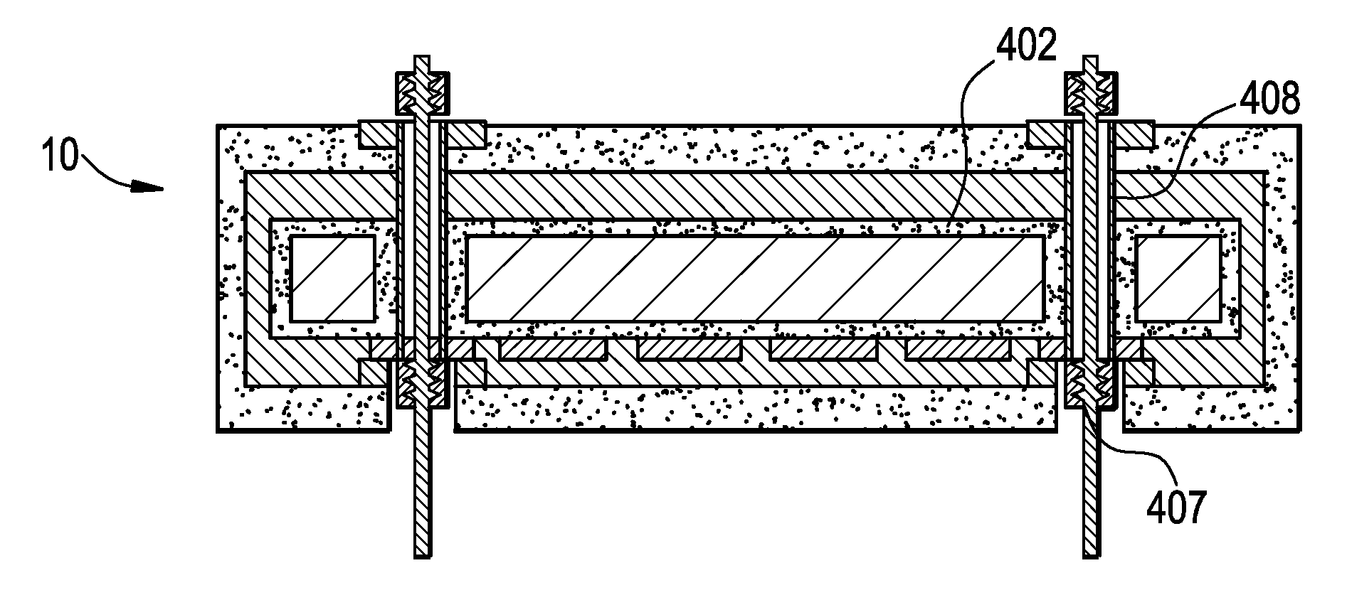
[0109]An electrically conductive heating element (molybdenum manganese) was deposited onto a ceramic substrate (AlN). The substrate contained through-holes to allow for installation of electrical contacts. In the next step, Ni-plated molybdenum posts were installed using molybdenum fasteners. The adhesive of Example 1 was painted around the contact points between the Ni-plated molybdenum posts, the molybdenum fasteners, heating element on the AlN substrate, and the AlN substrate. Next, the entire heater assembly including the contact was coated with AlN through a CVD process.

[0110]In a test simulating conditions of a heater with AlN substrate in a semiconductor processing environment, corrosion testing of the heater and contact was conducted after 100 thermal cycles between 400 and 500° C. at a ramp rate of 45° C. / min. In another test, a heater with graphite core was cycled 100 times between 400 and 600° C. with a ramp rate of 60° C. / min. The tests were to determine whether the gla...

example 3

[0113]A filler composition comprising a powder mixture from reagent grade raw materials in the amount of 45 wt % yttrium oxide, 20 wt % aluminum oxide, 35 wt % silicon dioxide was compared with other materials known in the art, including alumina, molybdenum, TaC, AlN, graphite, and nickel. In the test, a) dimensions and mass of the sample was measured prior to testing; b) parts were placed in a vacuum chamber, which is then pumped down to a pressure of approximately 1 millitorr; c) the parts were heated to the desired testing temperature; d) a fluorine / argon plasma was generated above parts for the desired time period; e) after testing, the parts were removed from the chamber and the mass after exposure was recorded. The corrosion rate is calculated as follows:

corrosion rate=mass loss / density / exposed surface area / time;

wherein a negative corrosion rates indicate mass gain after exposure, which translates to excellent corrosion resistance.

[0114]The results of the experiments comparing...


PUM

PropertyMeasurementUnit
temperatureaaaaaaaaaa
elongationaaaaaaaaaa
thicknessaaaaaaaaaa

Abstract

A wafer processing apparatus characterized by having corrosion resistant connections for its electrical connections, gas feed-through channels, recessed areas, raised areas, MESA, through-holes such as lift-pin holes, threaded bolt holes, blind holes, and the like, with the special configurations employing connectors and fillers having excellent chemical resistant properties and optimized CTEs, i.e., having a coefficient of thermal expansion (CTE) that closely matches the CTE of the base substrate layer, the electrode(s), as well as the CTE of coating layer. In one embodiment, a nickel plated molybdenum insert is employed.

Description

CROSS REFERENCE TO RELATED APPLICATION[0001]This application claims the benefits of U.S. 60 / 806648 filed Jul. 06, 2006, which patent application is fully incorporated herein by reference.FIELD OF INVENTION[0002]The invention relates generally to a wafer handling apparatus for use in the manufacture of semiconductors.BACKGROUND OF THE INVENTION[0003]The process for fabrication of electronic devices comprises a number of process steps that rely on either the controlled deposition or growth of materials or the controlled and often selective modification of previously deposited / grown materials. Exemplary processes include Chemical Vapor Deposition (CVD), Thermal Chemical Vapor Deposition (TCVD), Plasma Enhanced Chemical Vapor Deposition (PECVD), High Density Plasma Chemical Vapor Deposition (HDP CVD), Expanding Thermal Plasma Chemical Vapor Deposition (ETP CVD), Metal Organic Chemical Vapor Deposition (MOCVD), etc. In some of the processes such as CVD, one or more gaseous reactants are ...

Claims


Application Information

Patent Timeline
Patent Type & Authority Applications(United States)
IPC IPC(8): H01R43/00
CPCH01L21/67103H01L21/6875Y10T29/53213H01L21/68785H01L21/68757C03C3/062C03C4/20
Inventor OLECHNOWICZ, BENJAMIN J.RUSINKO, DAVID M.FAN, WEISARIGIANNIS, DEMETRIUSSCHAEPKENS, MARCLONGWORTH, DOUGLAS A.
Owner GENERAL ELECTRIC CO
Why Eureka
Try Eureka