Plasma Treatment Method and Plasma Etching Method

a plasma treatment and plasma technology, applied in the field of plasma treatment process, can solve the problems of damage to devices caused by plasma process, physical and chemical influence, etc., and achieve the effect of fine processing and high accuracy

Inactive Publication Date: 2008-04-10
SHOWA DENKO KK +1
View PDF7 Cites 241 Cited by
  • Summary
  • Abstract
  • Description
  • Claims
  • Application Information

AI Technical Summary

Benefits of technology

[0052] Using the plasma treatment process by use of a gas having no greenhouse effect according to the present invention, the plasma etching treatment with high accuracy suitable for fine processing in production of semiconductor devices can be attained. Particularly, from plasma, only neutral beams necessary for etching reaction are taken out and are irr

Problems solved by technology

Therefore, when the substrate is etched with radicals, etching progresses until the under part of an etching mask, that is, the mechanism (1) has a problem in that isotropic etching is performed.
The plasma process is necessary and indispensable as dry etching technique for semiconductors, however, damage on devices caused by the plasma process is induced in accordance with fining processing patterns.
Particularly, in highly technological processes such that processing patterns are fined to a size of not more than 0.1 μm, damage caused by irradiation with electric charges (electron, ion), light quantum (photon) and the like generated in plasma causes, for example, dielectric breakdown of a gate insulating film and abnormality of processing forms so that it exerts serious influences on device properties.
New materials called as high-k and low-k films have been actively studied and developed with the aim of enhancing the semiconductor device performance and saving electricity consumption, but they are physically and chemically unstable as compared with the silicon oxide (SiO2) films now in use so that it is considered that the damages caused by the plasma processing will be more remarkable.
As described above, fluorocarbon gas, however, has a problem of having a high global warming potential.
Consequently, the case of carrying out Si etching using conventional plasma processing has a problem in that when the F

Method used


Image

  • Plasma Treatment Method and Plasma Etching Method
  • Plasma Treatment Method and Plasma Etching Method
  • Plasma Treatment Method and Plasma Etching Method

Examples


example 1

[0365] Using a plasma and neutral beam analysis apparatus as shown in FIG. 4, a continuous plasma, pulse-time-modulated plasma and neutral beam were generated from fluorine gas (F2) and then the generated continuous plasma, pulse-time-modulated plasma and neutral beam were analyzed using QMS (quadrupole mass spectrometer), a microwave interferometer, an emission spectrometer, a Faraday cup and a calorimeter.

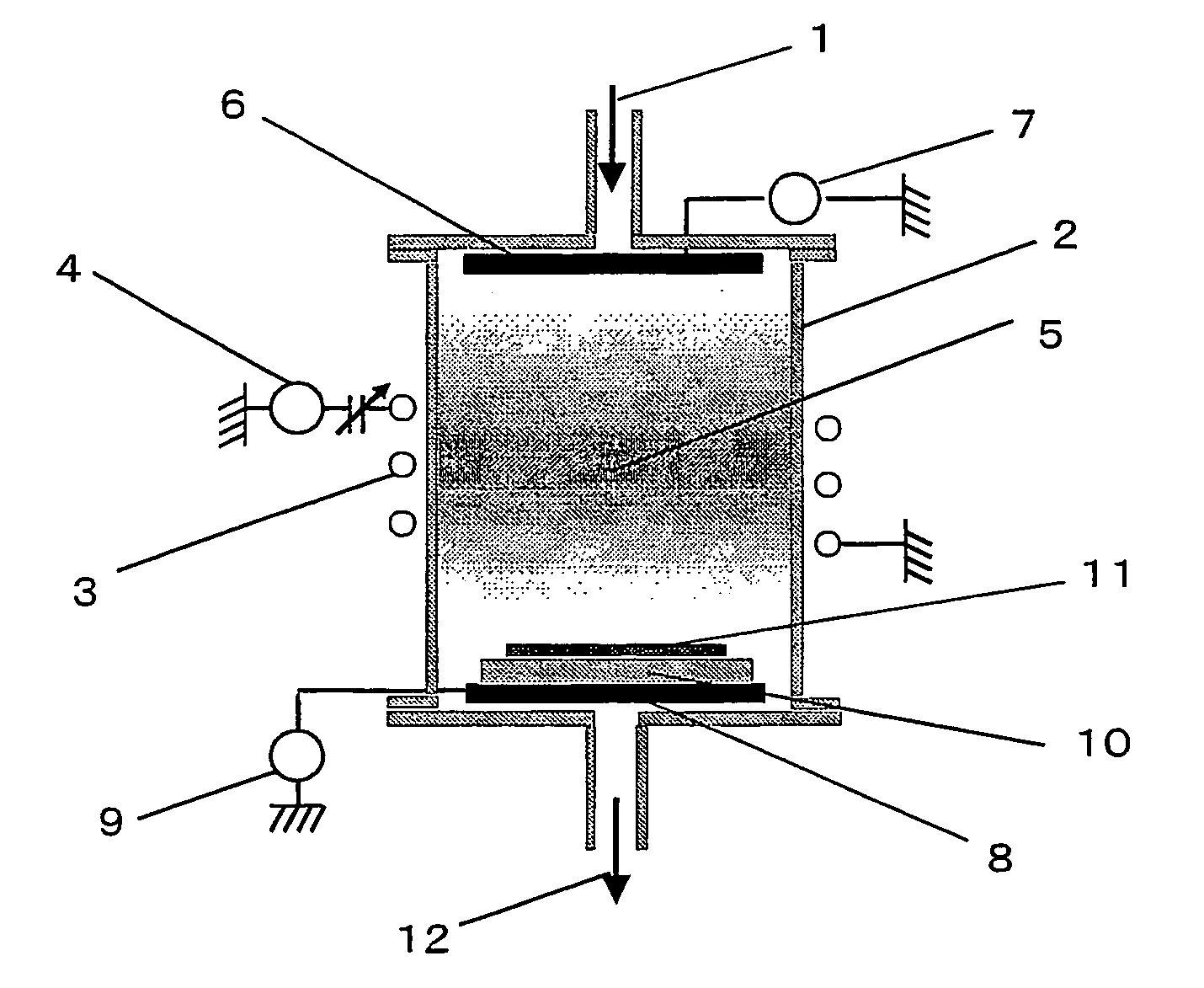
[0366] At first, the structure of the plasma and neutral beam analysis apparatus as shown in FIG. 4 is described below. In the plasma and neutral beam analysis apparatus as shown in FIG. 4, a quartz made plasma generating chamber 42 has the same structure as the quartz made plasma generating and substrate treatment chamber 2 in the pulse-time-modulated plasma generating apparatus as shown in FIG. 1. The plasma generating chamber 42 is provided with a port for feeding a treatment gas 41, and an antenna 43 for generating inductively coupled plasma is rolled up in a coil-like state...

example 2

[0393] Plasma etching for a substrate was carried out by a pulse-time-modulated plasma of fluorine gas (F2), the etching rate of silicon (Si) was measured and the etching form was observed.

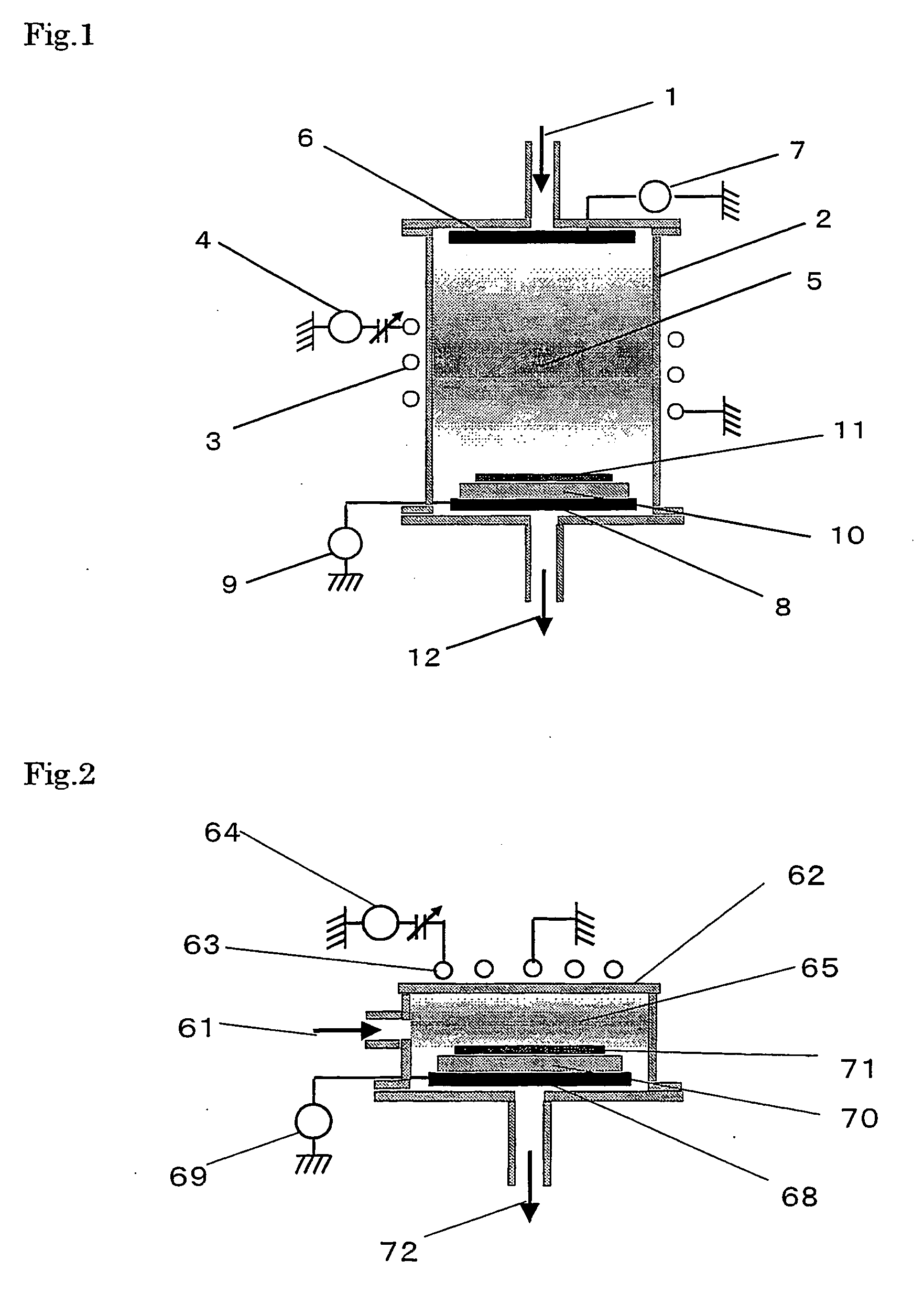
[0394] Using a pulse-time-modulated plasma generating apparatus as shown in FIG. 2, 30 mL / min of the 100% by volume fluorine gas (F2) same as one used in Example 1 was introduced as a treatment gas 61 into a plasma generating and substrate treatment chamber 62, and RF bias (1 kW) having a discharge frequency of 13.56 MHz was applied from a high frequency electric source 64 to an antenna 63 to generate a continuous plasma 65.

[0395] To a carbon made electrode for accelerating ion 68, RF bias of 1 MHz was applied with an output of 50 W from an electric source for applying voltage 69. By applying the RF bias to the carbon made electrode for accelerating ion 68 in this manner, positive and negative ions generated in the plasma 65 were accelerated in the direction almost vertical to a substrate holdin...

example 3

[0399] From pulse-time-modulated plasma of fluorine gas (F2), negative ions were selectively extracted and neutralized to generate a neutral beam. By the neutral beam, plasma etching of a substrate was carried out. In order to examine the composition of the neutral beam, etching rates of polysilicon (Poly-Si) and SiO2 were measured using electrodes of extracting beams having a different F radical-adhering coefficient, and further the etching form of Poly-Si was observed.

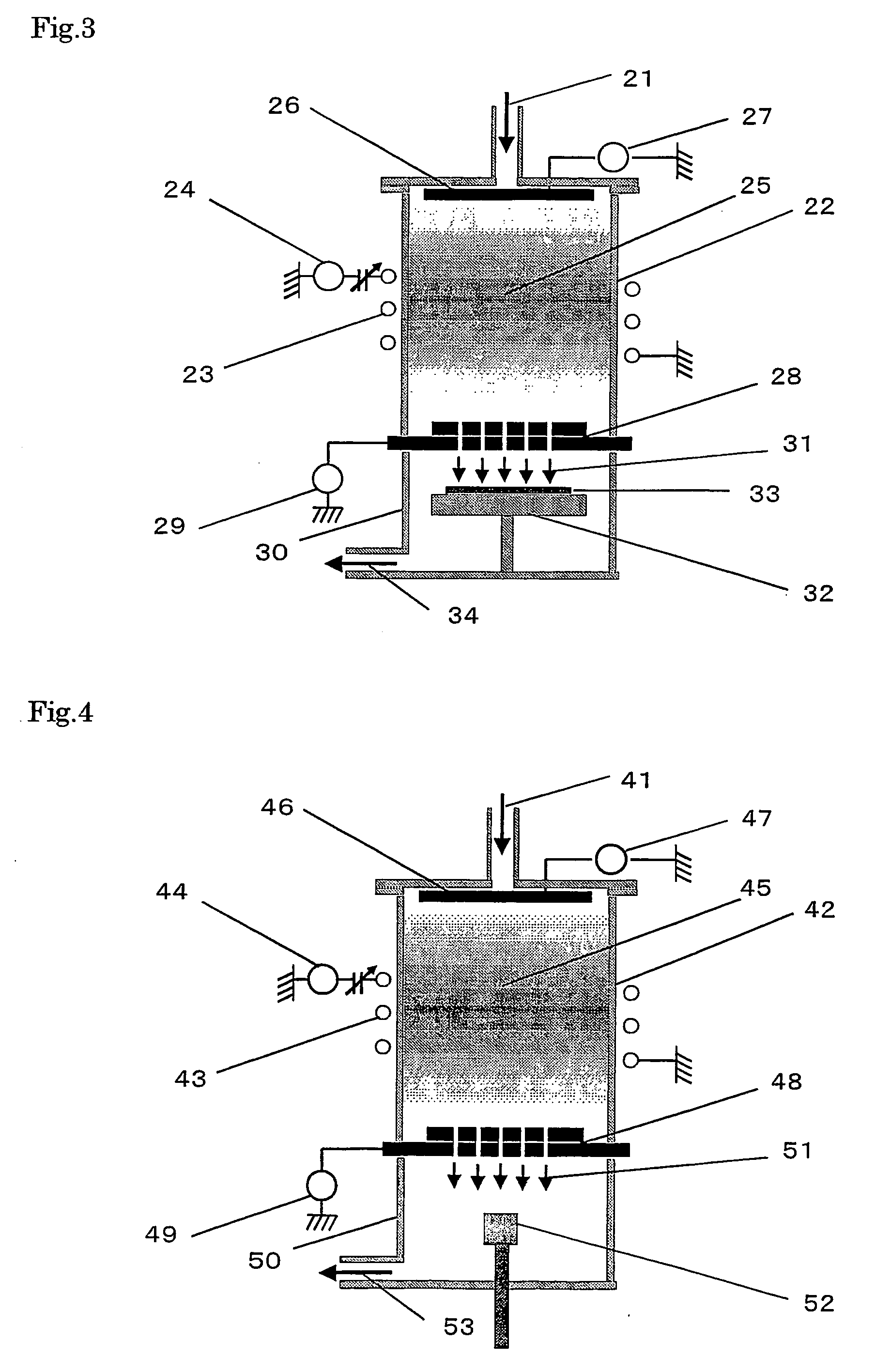
[0400] Using the neutral beam generating apparatus as shown in FIG. 3, 30 mL / min of the 100% by volume fluorine gas (F2) same as that used in Example 1 was introduced as a treatment gas 21 to a plasma generating chamber 22, and RF bias of 1 kW having a discharge frequency of 13.56 MHz (during the ON time) was applied in a pulse state from a high frequency electric source 24 to an antenna 23, to generate pulse-time-modulated plasma. In this procedure, the ON time / OFF time in the pulse-time-modulation were 50 μsec / 50 ...


PUM


Abstract

The present invention develops a process for plasma treatment using a gas having no greenhouse effect in order to realize global environmental preservation and sophistication of plasma process performance and provides a process for plasma etching with high accuracy which process can depress damage to devices. The process for plasma treatment according to the present invention comprises the steps of feeding a treatment gas containing fluorine gas (F2) into a plasma generating chamber, alternately repeating application of high frequency electric field and stop of the application thereof to generate plasma, and carrying out substrate treatment by irradiating the plasma to a substrate. Furthermore, the substrate treatment may be carried out by individually or alternately extracting negative ions or positive ions from the plasma, or selectively extracting only negative ions, neutralizing them, to generate a neutral beam and irradiating the neutral beam to the substrate.

Description

CROSS REFERENCES OF RELATED APPLICATION [0001] This application is an application filed under 35 U.S.C. §111(a) claiming benefit pursuant to 35 U.S.C. §119(e) of the filing date of Provisional Application 60 / 589, 574 filed on Jul. 21, 2004, pursuant to 35 U.S.C. §111(b).TECHNICAL FIELD [0002] The present invention relates to a plasma treatment process for treating a substrate using plasma generated utilizing a high frequency electric field, and relates to a plasma etching process suitable for fine processing in production of semiconductor elements and micro machine (MEMS: Micro Electric Mechanical System) elements. TECHNICAL BACKGROUND [0003] In plasma processes used for dry etching during the production processes of semiconductor integrated circuits, large amounts of fluorocarbon type or inorganic fluoride type gases, (for example, carbon tetrafluoride gas (CF4), sulfur hexafluoride gas (SF6), or the like) are used. However, the fluorocarbon type and inorganic fluoride type gases a...

Claims


Application Information

Patent Timeline
IPC IPC(8): H01L21/302H01L21/3065H01L21/311H01L21/3213
CPCH01L21/3065H01L21/32137H01L21/31116
Inventor HOSHINO, YASUYUKISAMUKAWA, SEIJI
Owner SHOWA DENKO KK
Why Eureka
Try Eureka