

Laser irradiation apparatus, laser irradiation method, and method for manufacturing a semiconductor device
a laser irradiation and semiconductor technology, applied in the field of laser irradiation apparatus, laser irradiation method, and method for manufacturing a semiconductor device, can solve the problems of lowering the transporting characteristic of the carrier, difficult to enhance the throughput, and the nonlinear optical element converting the laser light into the harmonic does not have enough resistance to the laser light, so as to achieve enhanced laser crystallization throughput, the effect of increasing the fundamental wave absorption coefficien
- Summary
- Abstract
- Description
- Claims
- Application Information
AI Technical Summary
Benefits of technology
Problems solved by technology
Method used
Image

Examples
embodiment mode 1
[0069]The structure of the laser irradiation apparatus of the present invention is explained with reference to FIG. 3.
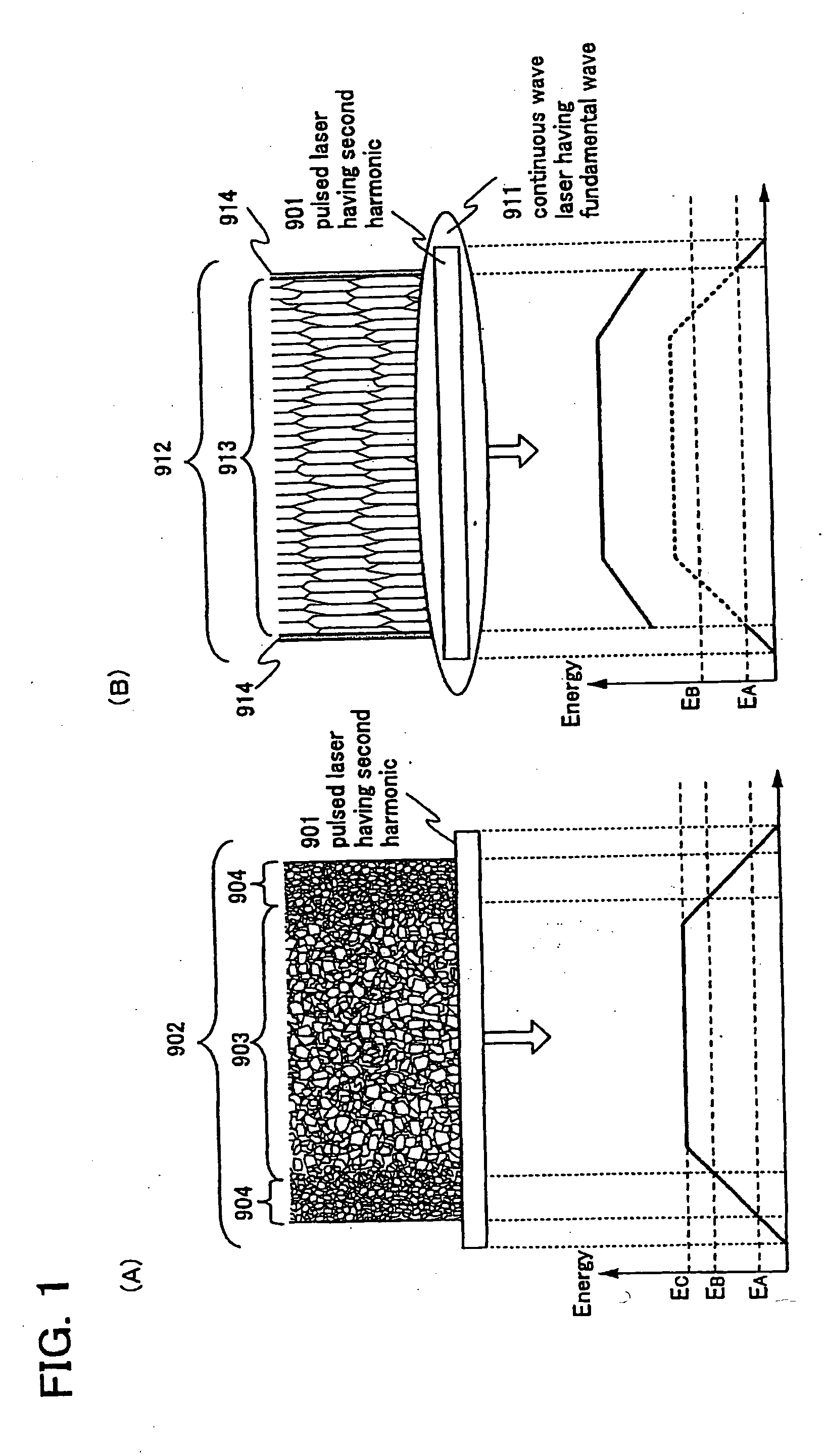
[0070]A reference numeral 101 denotes a pulsed laser oscillator and a Nd: YLF laser having an output of 6 W is used in the present embodiment mode. The laser oscillator 101 has an oscillation mode of TEM00 and the laser light is converted into the second harmonic by a nonlinear optical element. Although it is not in particular necessary to limit to the second harmonic, the second harmonic is superior to the other higher harmonic in terms of energy efficiency. The frequency is 1 kHz and the pulse width is approximately 60 nsec. Although the solid-state laser with an output of approximately 6 W is employed in the present embodiment mode, a large-scale laser having an output as much as 300 W such as a XeCl excimer laser, a KrF excimer laser, or an ArF excimer laser may be also employed. For example, the XeCl excimer laser has a wavelength of 308 nm and the KrF excimer l...
embodiment mode 2
[0100]A laser light irradiation method and a method for manufacturing a semiconductor device of the present invention are explained with reference to FIG. 9.
[0101]First of all, a base film 501 is formed on a substrate 500 as shown in FIG. 9(A). A glass substrate such as a barium borosilicate glass or an aluminum borosilicate glass, a quartz substrate, an SUS substrate, or the like can be used as the substrate 500. In addition, although the substrate made of flexible synthetic resin such as acryl or plastic typified by PET, PES, or PEN is inferior to the above substrate in terms of the resistance against the heat, the substrate made of flexible synthetic resin can be utilized when it can resist against the heat generated in the manufacturing process.
[0102]The base film 501 is provided in order to prevent that alkaline-earth metal or alkaline metal such as Na included in the substrate 500 diffuses to the semiconductor film to have an adverse affect on the characteristic of a semicondu...
embodiment 1
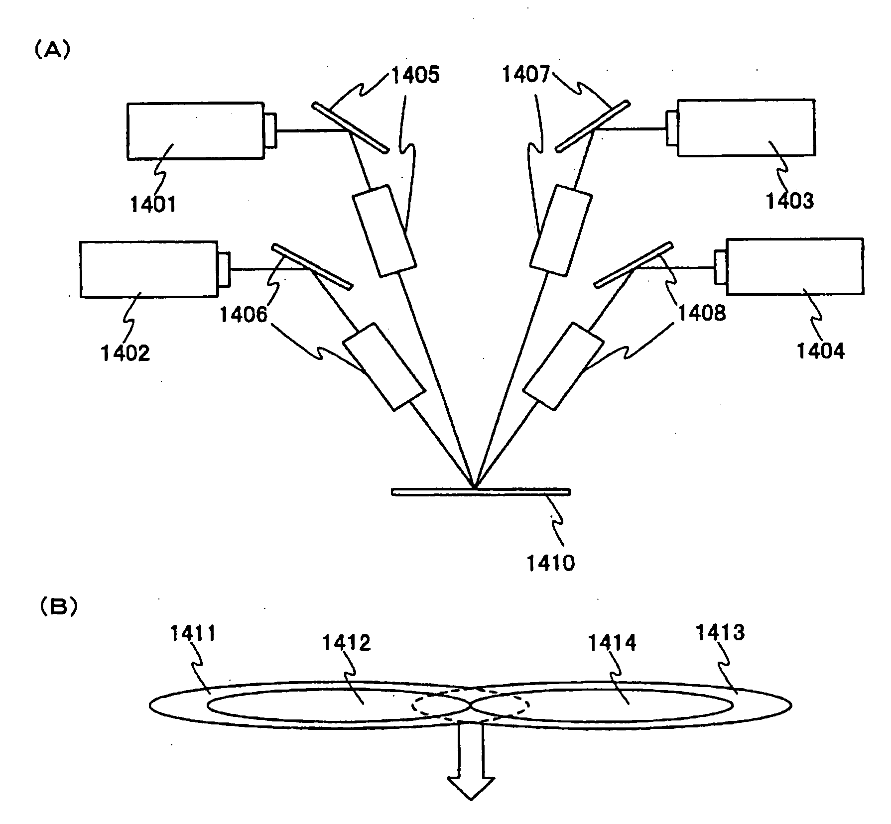
[0123]This embodiment explains one mode of the laser irradiation apparatus of the present invention.
[0124]FIG. 5 shows a structure of the laser irradiation apparatus of this embodiment. In this embodiment, first laser light having a wavelength not longer than that of the visible light is generated in a pulse oscillation from a laser oscillator 1520. And second laser light are generated in a continuous wave oscillation from two laser oscillators 1500 and 1501.
[0125]In this embodiment, an excimer laser is used as the laser oscillator 1520. The output power per a pulse is set to 1 J, and the pulse width is set to approximately 30 nsec, that is to say, the output per unit of time is set to 30 MW. In addition, both of the laser oscillators 1500 and 1501 are YAG lasers in which the output energy is set to 10 kW respectively.
[0126]After the first laser light emitted from the laser oscillator 1520 is reflected by a mirror 1523, the first laser light is shaped into rectangular, elliptical, o...
PUM
| Property | Measurement | Unit |
|---|---|---|
| length | aaaaa | aaaaa |
| aspect ratio | aaaaa | aaaaa |
| aspect ratio | aaaaa | aaaaa |
Abstract
Description
Claims
Application Information