Integrated optics arrangement for wavelength (De)multiplexing in a multi-grade vertical stack

Active Publication Date: 2008-06-12
ONECHIP PHOTONICS
View PDF7 Cites 18 Cited by
  • Summary
  • Abstract
  • Description
  • Claims
  • Application Information

AI Technical Summary

Benefits of technology

[0027]In the fourth exemplary embodiment of the two-wavelength VWM, the first designated waveguide is the edge-emitting semiconductor injection laser and the second designated waveguide is the photodetector, therefore enabling for the monolithically integrated bidirectional transceiver, in which outgoing optical signals are transmitted in the shorter wavelength and incoming optical signals are received in the longer wavelength. In the particular case of λ

Problems solved by technology

In recent years, we have been witnessing a rapid advancement of the optical access and local area networks driven by ever growing bandwidth demand, and fundamental inability of the competing technologies, e.g. those based on twisted copper, coaxial cable or wireless transmission, to deliver.
Deep penetration of the optical fiber into the access networks requires an unparalleled massive deployment of the optical gear that drives the traffic to and from the Internet users.
Therefore, cost efficiency and volume scalability in manufacturing of such components are increasingly becoming the major issues.
Within a framework of the current optical component manufacturing paradigm, which is based mainly on bulk optical sub-assemblies (OSA) from off-the-shelf discrete passive and active photonic devices, the root cause of the problem is in a labor-intensive optical alignment and costly multiple packaging.
Not only do these limit the cost efficiency, but also significantly restrict the manufacturer's ability of ramping volume and providing scalability in manufacturing.
On a flip side, the design of PICs based on the MGVI platform is challenging because of a necessity for organizing of functionally different waveguide elements at different vertical levels of the MGVI structure into a common optical circuit, through a controllable transition of the optical signals between vertically stacked optical waveguides.
The problem is further complicated then the PIC operates in a plurality of wavelengths, each of which i

Method used


Image

  • Integrated optics arrangement for wavelength (De)multiplexing in a multi-grade vertical stack
  • Integrated optics arrangement for wavelength (De)multiplexing in a multi-grade vertical stack
  • Integrated optics arrangement for wavelength (De)multiplexing in a multi-grade vertical stack

Examples


first embodiment

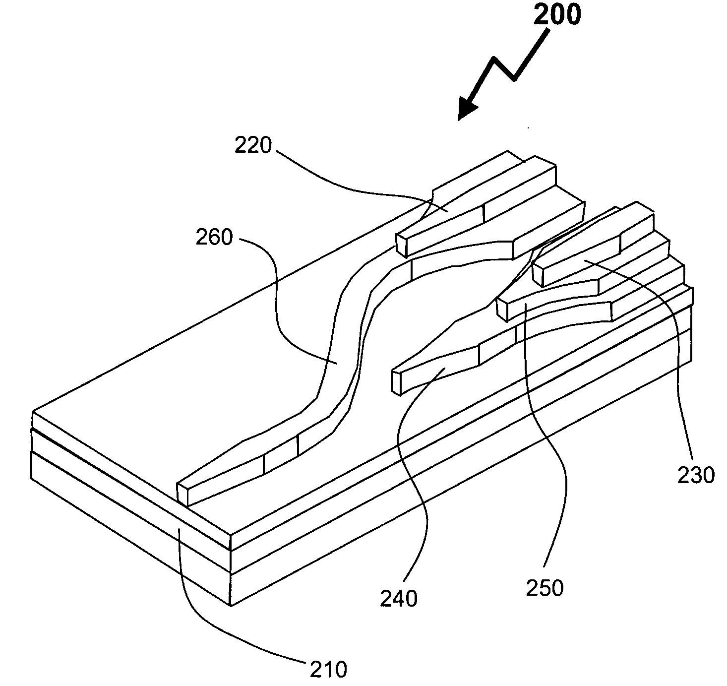
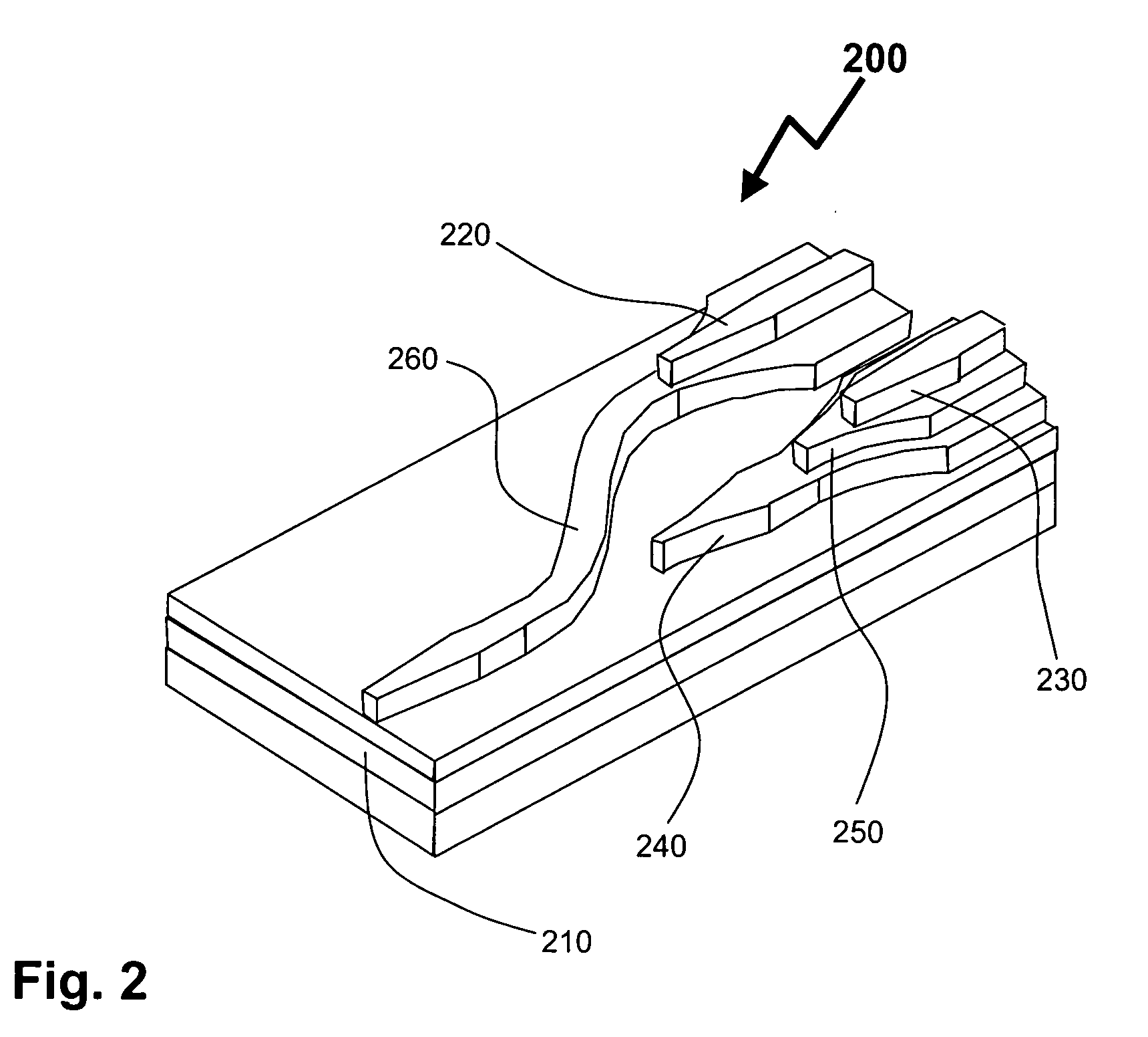
[0043]The solution to this problem is illustrated by FIG. 2, which gives a schematic three-dimensional view of the present invention in the form of two-wavelength VWM 200 having one common waveguide and two wavelength-designated waveguides. Whereas the bottom part of this waveguide arrangement is similar to that of the previous art, shown in FIG. 1, there is a fundamental difference in design and operating principle between the two.

[0044]Design-wise, the MGVI structure is different in that the guiding layer of the first designated waveguide is now composed of two layers, each capable of supporting the guided mode in the first operating wavelength, of which the lower core layer is transparent for this wavelength (i.e. made up from the semiconductor material having the bandgap wavelength well above the first operating wavelength). Another design difference is in that the waveguide router is formed in the lower core of the guiding layer of the first designated waveguide is lateral, suc...

second embodiment

[0061]FIG. 5 illustrates the second embodiment related to the lateral router aspect of the invention, in which the waveguide bend section of the transition waveguide 510c of a two-wavelength VWM 500 is complemented with a curved deep trench 510d, etched in the proximity of the waveguide bending, such that, in use, it provides an additional lateral confinement to the waveguide mode propagating therein and, therefore, reduces its leakage from the bended section of the transition waveguide, therefore, improving the insertion loss for the first wavelength. A combination of the sharp waveguide bending and curved trench, similar to that shown in FIG. 5, has been proven in the previous art to be an efficient solution to a leakage problem occurring at the waveguide bend, see for example Seo et al. (“Low Transition Losses in Bent Rib Waveguides”, J. Lightwave Technology, Vol. 14, No. 10, PP. 2255-2259, 1996). Further improvements of the same nature can be achieved by adding continues / segment...

third embodiment

[0062]Now referring to FIG. 6, illustrated is the lateral router aspect of the invention, in which the lateral re-direction of the first wavelength still is achieved by bending the transition waveguide 610c, but a lateral ARROW structure 610e through 610g defined by semiconductor etching process next to the waveguide bend is employed as an additional feature serving to reduce the leakage of the optical mode from the bended section of the transition waveguide. The design and operating principles of the ARROW structures 610e through 610g are well described in the previous art, see for example Galarza, et al (“Simple low-loss waveguide bends using ARROW effect”, Appl. Physics B, Vol. 80, PP. 745-748, 2005). Bended lateral ARROW structure added on the outer side of the waveguide bend allows for higher bending curvature without extra loss, therefore, enabling for smaller footprint designs.


PUM


Abstract

The invention describes an integrated-photonics arrangement, implementable in a multi-guide vertical integration structure composed from III-V semiconductors and grown in one epitaxial growth run, that allows for vertical and lateral splitting of optical signals co- or bi-directionally propagating in the common passive waveguide into plurality of the vertically integrated passive or active wavelength-designated waveguides, therefore, enabling the wavelength-designated waveguides operating in different wavelengths to be monolithically integrated onto the same substrate and connected to the shared passive waveguide. In the exemplary embodiments of the invention, two active wavelength-designated waveguides, each of which either laser or photodetector, are vertically integrated with a common passive waveguide connected to the input/output optical port shared by both operating wavelengths, to form a single-fiber, two-wavelength receiver (both wavelength-designated waveguides are waveguide photodetectors) or transmitter (both wavelength-designated waveguides are edge-emitting semiconductor injection lasers) or transceiver (one wavelength-designated waveguide is waveguide photodetector and the other—edge-emitting semiconductor injection laser). Advantageously to the previous art, the proposed vertical splitting and lateral routing allows for a reduced footprint size while greatly improving design flexibility and/or device performance.

Description

[0001]This application claims the benefit of U.S. Provisional Patent Application No. 60 / 860,221 filed Nov. 21, 2006, the entire contents of which are incorporated herein by reference.FIELD OF THE INVENTION[0002]The invention relates generally to the field of integrated photonics, and more particularly to wavelength division multiplexing (WDM) in photonic integrated circuits (PICs) in III-V compound semiconductor materials.BACKGROUND OF THE INVENTION[0003]In recent years, we have been witnessing a rapid advancement of the optical access and local area networks driven by ever growing bandwidth demand, and fundamental inability of the competing technologies, e.g. those based on twisted copper, coaxial cable or wireless transmission, to deliver. Transmission over optical fiber is emerging as a universal means for communications, from long-haul to metropolitan area to broadband access networks, resulting in an explosion of optical Internet and convergence of different media streams (e.g....

Claims


Application Information

Patent Timeline
IPC IPC(8): G02B6/12
CPCG02B6/1228G02B2006/12119G02B2006/12097G02B6/125
Inventor TOLSTIKHIN, VALERYLOGVIN, YURYPIMENOV, KIRILL
Owner ONECHIP PHOTONICS
Why Eureka
Try Eureka