Micro-electro mechanical device made from mono-crystalline silicon and method of manufacture therefore

a mono-crystalline silicon and micro-electromechanical technology, applied in the direction of microstructural technology, semiconductor/solid-state device manufacturing, electric devices, etc., can solve the problems of not able to withstand high temperature anneal, both dimension control and contamination control are major challenges, and the movable element deformation is not easy to be distorted, so as to improve the performance of micro-electro-mechanical inertial sensors

Inactive Publication Date: 2008-06-12
WAN CHANG FENG
View PDF2 Cites 59 Cited by
  • Summary
  • Abstract
  • Description
  • Claims
  • Application Information

AI Technical Summary

Benefits of technology

[0017]It is one object of the present invention to improve the performance of

Problems solved by technology

Conversely, an electrical signal applied to the capacitive plates or piezoelectric layers can result in deflection in the movable elements.
This is normally done by anisotropic wet etch where both dimension control and contamination control is a major challenge.
Polymer bonding is attractive because it is widely used in attaching semiconductor dies to substrates for packaging, but it is rarely used in micro-machining as most of these applications require very thin bondlines.
The application of a thin layer of polymer adhesive requires thinning with solvent that is incompatible with most micro-machining techniques.
Photoresist can be dry etched in oxygen plasma but can not withstand high temperature anneal like silicon dioxide can.
Unfortunately, it must be annealed at a high temperature (˜1000° C.) to reduce stress, or its suspended structure will curl after the sacrificial layer is removed from underneath.
To separate them without causing damage is difficult because the combination of adhesive forces and electrostatic forces is large compared to the strength of the thin films.
Another drawback is that the metal interconnect in the integrated control circuits cannot withstand the high temperature anneal.
Protecting the suspended structure during the interconnect process and the wet etch is a complex matter and entails the usage of costly state-of-the-art fabrication facilities.
However, the intrinsic stress and hysteresis in the deposited film limits its thickness to a few thousand angstroms or the films can curl and change after stressing.
This makes the technique not suitable for devices such as accelerometers that require larger proof mass.
However, SOI wafers are much more expensive than the regular wafers and its production employs a high temperature process that is not compatible with integrated circuits and dry-etchable sacrificial layers.
Another issue related to non-dry-etchable sacrificial layers r

Method used


Image

  • Micro-electro mechanical device made from mono-crystalline silicon and method of manufacture therefore
  • Micro-electro mechanical device made from mono-crystalline silicon and method of manufacture therefore
  • Micro-electro mechanical device made from mono-crystalline silicon and method of manufacture therefore

Examples


Embodiment Construction

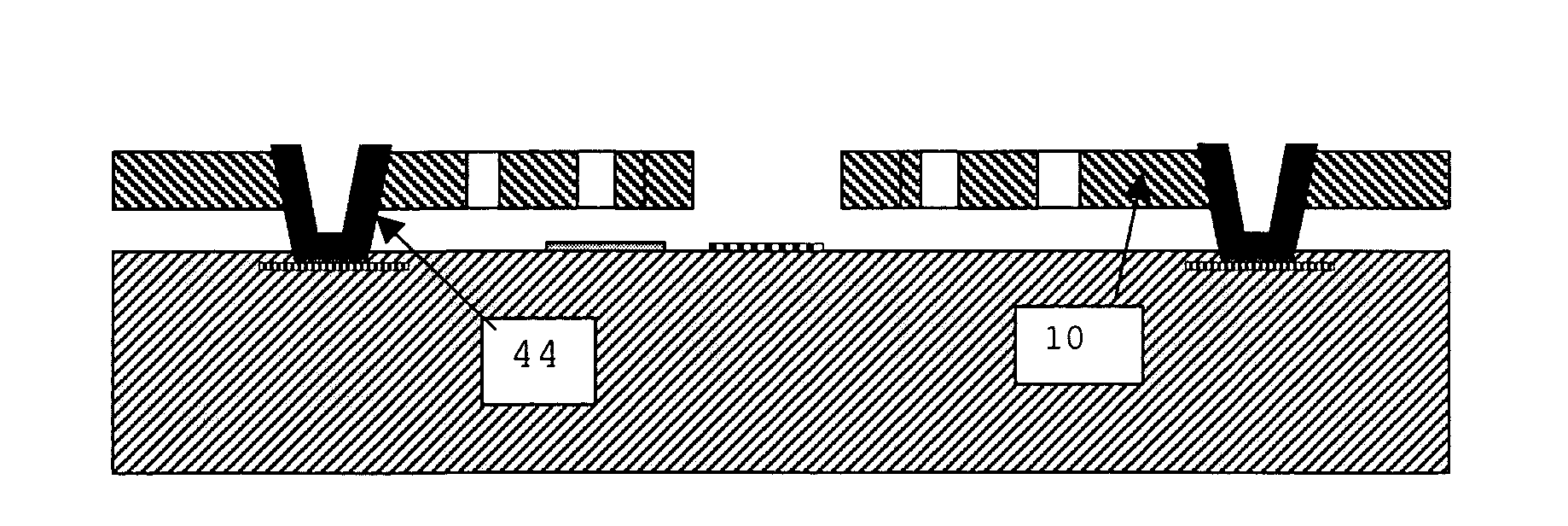
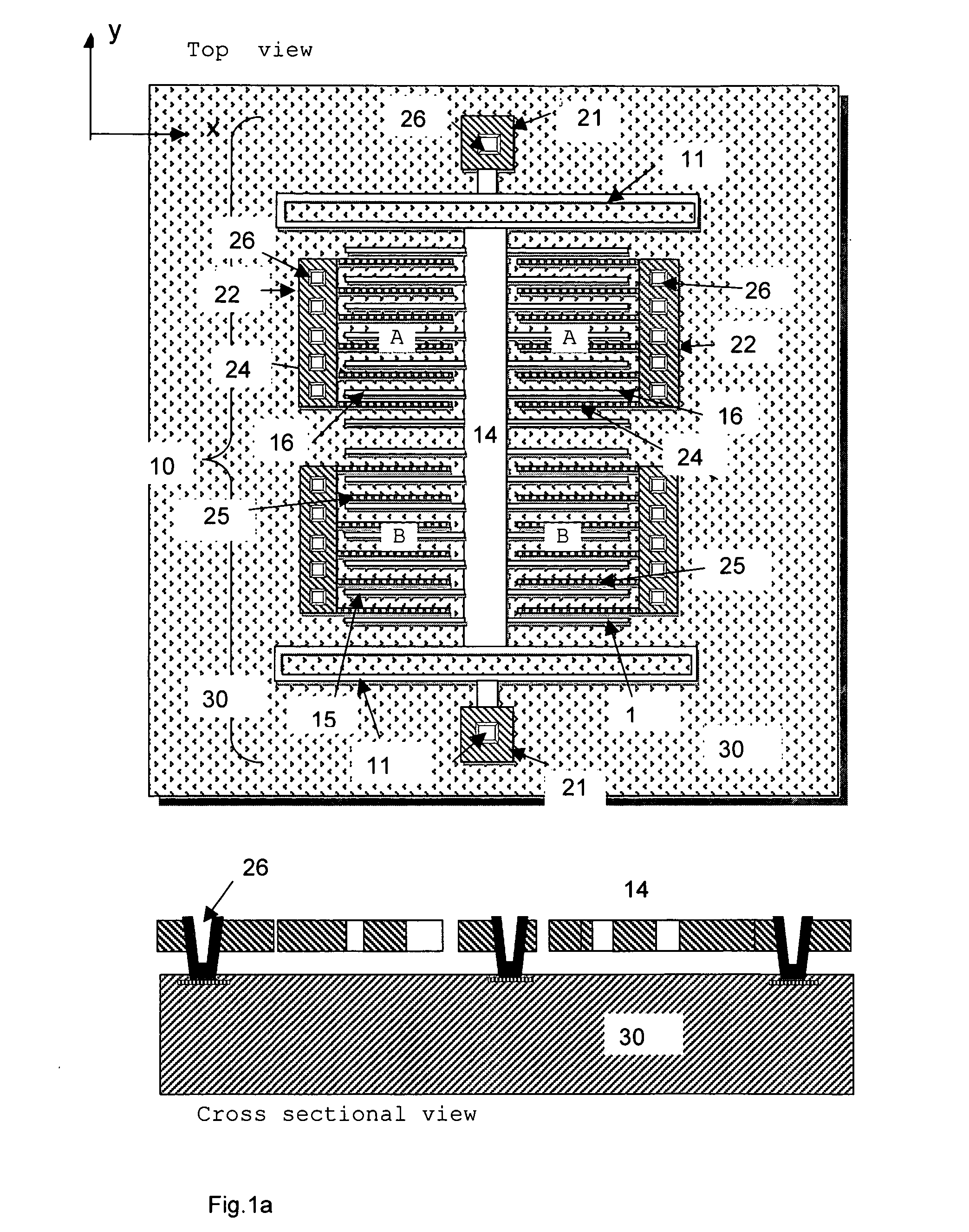
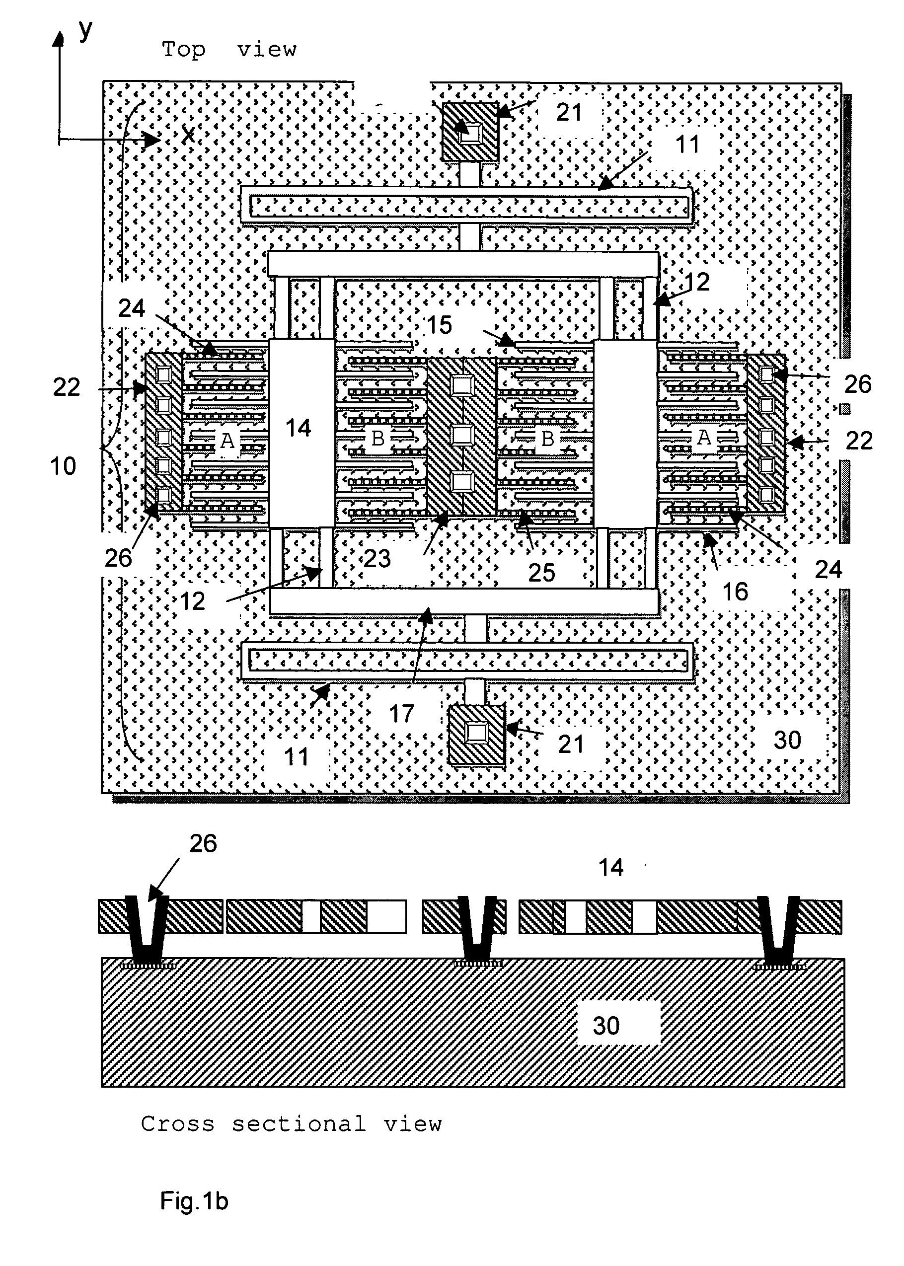
[0046]Reference is made to FIG. 1a, wherein an accelerometer embodiment of the present invention is depicted, in both a top view and a cross sectional view. This accelerometer MEMS device comprises suspended structures 10, anchored on a substrate 30, which is shown as the large rectangle in the background. The suspended structure is fabricated from a doped mono-crystalline silicon wafer; the substrate comprises electrical components, such as signal processing integrated circuitry, metal landing pads, metal strips and capacitive plates. The suspended structure 10 comprises movable elements and stationary elements. The movable elements include proof mass 14, having a movable, rectangular beam and a plurality of fingers 15 and 16 extending from both sides, and two flexure springs 11, which connect each end of the proof mass 14 to anchors. The stationary elements include anchoring plates 21 and 22 which fasten the suspended structures to the substrate 30, a plurality of stationary finge...


PUM


Abstract

The present invention is related to a method for manufacturing micro-electro-mechanical systems (MEMS) having movable and stationary suspended structures formed from mono-crystalline silicon wafer or chip, bonded to a substrate wafer with an polymer adhesive layer that serves as spacer and as a sacrificial layer which is undercut by dry etch means. The substrate wafer contains electronic circuits for sensing and actuating the suspended structure by electrical means. Electrical interconnections between the suspended structures and the substrate can be made by etching through via holes in the suspended structure and the adhesive, depositing metal layers in the via holes, and removing the metal layers from outside the via holes. The metal layers in the via holes can also be used as pillars for supporting the suspended structures. This method can be used to manufacture inertial sensors.

Description

CROSS REFERENCE TO RELATED APPLICATION[0001]This continuation-in-part application claims the benefit of patent application Ser. No. 09 / 461,018, filed Dec. 15, 1999 and entitled “A MICRO-ELECTRO MECHANICAL DEVICE MADE FROM MONO-CRYSTALLINE SILICON AND METHOD OF MANUFACTURE THEREFORE.”BACKGROUND OF THE INVENTION[0002]1. Technical Field of the Invention[0003]The present invention relates to a micromachining process that is compatible with dry-etchable sacrificial layers, thick mono-crystalline suspended layers, on-chip electronics on the substrate and, in particular, to a interconnect between the thick mono-crystalline suspended layers and the microelectronics on the substrate.[0004]2. Description of the Related Art[0005]A micro-electro-mechanical system (MEMS) is a device that transforms mechanical activity into electrical signals and vice versa. A key element in MEMS is a variable capacitor formed between a stationary electrode and a movable electrode attached to a suspended proof ma...

Claims


Application Information

Patent Timeline
IPC IPC(8): H01L21/30
CPCB81B2203/0118B81B2203/0307B81C2201/019B81C1/00095B81B2207/07
Inventor WAN, CHANG-FENG
Owner WAN CHANG FENG
Why Eureka
Try Eureka