High performance devices enabled by epitaxial, preferentially oriented, nanodots and/or nanorods

a technology of epitaxial and nanorods, applied in the direction of superconducting magnets/coils, instruments, magnetic bodies, etc., can solve the problems of inability to retain the magnetization applied to the bit against thermal decay, current media will encounter a physical limit, and the least difficult to achieve. achieve the effect of high performan

Active Publication Date: 2008-07-24
GOYAL AMIT
View PDF3 Cites 69 Cited by
  • Summary
  • Abstract
  • Description
  • Claims
  • Application Information

AI Technical Summary

Benefits of technology

[0014]In accordance with one aspect of the present invention, the foregoing and other objects are achieved by fabrication of self-assembled, crystalline nanodots and nanorods of a certain composition within a crystalline matrix of another phase. As used herein, the phrase “self-assembled” is defined herein to mean a self-ordering process wherein the ordering occurs naturally during growth of the composite material or film. In particular, the invention enables fabrication of high performance and novel, electrical, magnetic, electromagnetic and electrooptical devices via epitaxial deposition on single crystal and / or single crystal-like, biaxially textured substrates by incorporation of self-assembled nanodots and nanorods of a second phase material within a device layer.

Problems solved by technology

It has been predicted that current media will encounter a physical limit which will prevent, or at least make very difficult, the manufacture of high-density magnetic storage media with an areal density of over 200-300 Gbit / in2.
However, if the grain size is too small, the magnetization applied to the bit cannot be retained against thermal decay due to the very small energy barrier height.
As a consequence, applied magnetization would be able to switch easily, and thus recorded data could be lost.
However, no method exists which can readily produce three dimensionally ordered bits and hence these have yet to be shown possible.
Thus, the challenge in realizing quantum dot lasers with operation significantly superior to that shown by quantum well lasers is that of forming high quality, uniform quantum dots in the active layer.
It is well known that defects within superconducting materials can pin the magnetic flux lines so that large currents can flow through the materials in the presence of high applied magnetic fields.
However, the density of these naturally formed defects is not high enough to provide the necessary performance requirements for the various applications in question.
These columnar defects leave amorphized damage tracks in the superconductor.
This approach, however, is not practical for scale-up as it is not only too expensive but can render the metallic substrate radioactive.
These substrates however cannot be fabricated in long lengths or in large area and essentially limited to sizes of about a foot in length and diameter at best.

Method used


Image

  • High performance devices enabled by epitaxial, preferentially oriented, nanodots and/or nanorods
  • High performance devices enabled by epitaxial, preferentially oriented, nanodots and/or nanorods
  • High performance devices enabled by epitaxial, preferentially oriented, nanodots and/or nanorods

Examples


example 1

[0050]Self-assembled nanodots and nanorods of non-superconducting phases were incorporated by performing laser ablation from a single target comprising a mixture of YBCO powder and nanoparticles of the chosen non-superconducting phase. Nanoparticles of materials such as BZO, CaZrO3 (CZO), YSZ, BaxSr1−xTiO3 (BST), etc. are commercially available from vendors such as Sigma-Aldrich. These nanoparticles, with a sharp particle size distribution ranging from 10-100 nm, are well-mixed with YBCO powder, via mechanical mixing, then cold pressed to form a green target. The target was then sintered at 950° C. in flowing oxygen. The target is then mounted on the target holder in the pulsed laser deposition (PLD) experimental setup. Depositions were performed on the technically important rolling-assisted-biaxially-textured-substrates (RABiTS) substrates with the configuration Ni-5 at % W (50 μm) / Y2O3 (75 nm) / YSZ (75 nm) / CeO2 (75 nm). PLD depositions were performed using a XeCl (308 nm) excimer l...

example 2

[0055]A 3 μm thick YBCO composite film containing self-assembled nanodots of BZO was prepared by pulsed laser deposition (PLD) using a XeCl (λ=308 nm) excimer laser at a repetition rate of 10 Hz. The 2-vol % BaZrO3-YBCO PLD target (1 inch diameter, 0.25 inch thick) was made by mixing YBCO powder and commercially available BaZrO3 nanopowder. The growth temperature was 790° C. and the base chamber pressure was 2×10⁻⁶ Torr with an oxygen partial pressure of 230 mTorr. All depositions were performed in a stationery configuration on the technically important RABiTS substrates with the configuration Ni-3 at % W (50 μm) / Y2O3 (65 nm) / YSZ (185 nm) / CeO2 (30 nm). The Y2O3 layer was deposited using e-beam evaporation and YSZ and CeO2 layers were deposited using rf-sputtering. The standard four-point probe method with a voltage criterion of 1 μV / cm was used for the transport measurements. Cross-section transmission electron microscopy (TEM) was used for microstructural analysis using a Hitachi H...

example 3

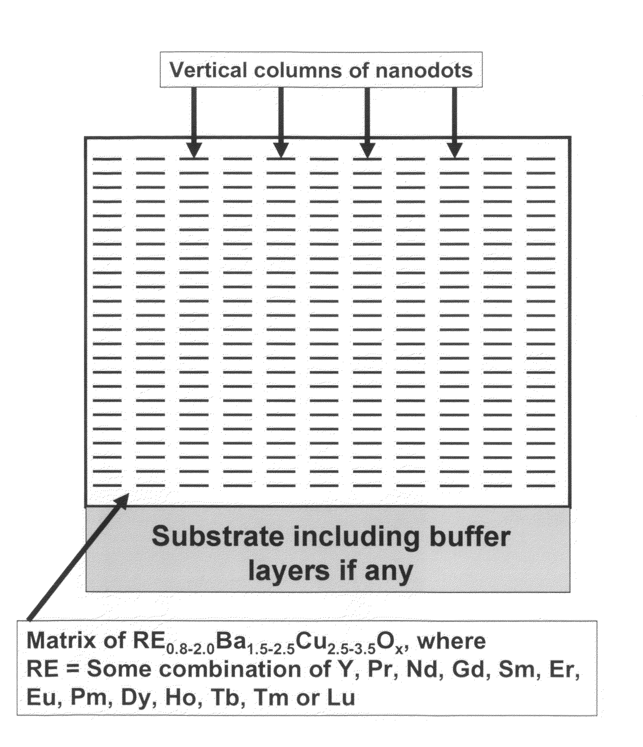
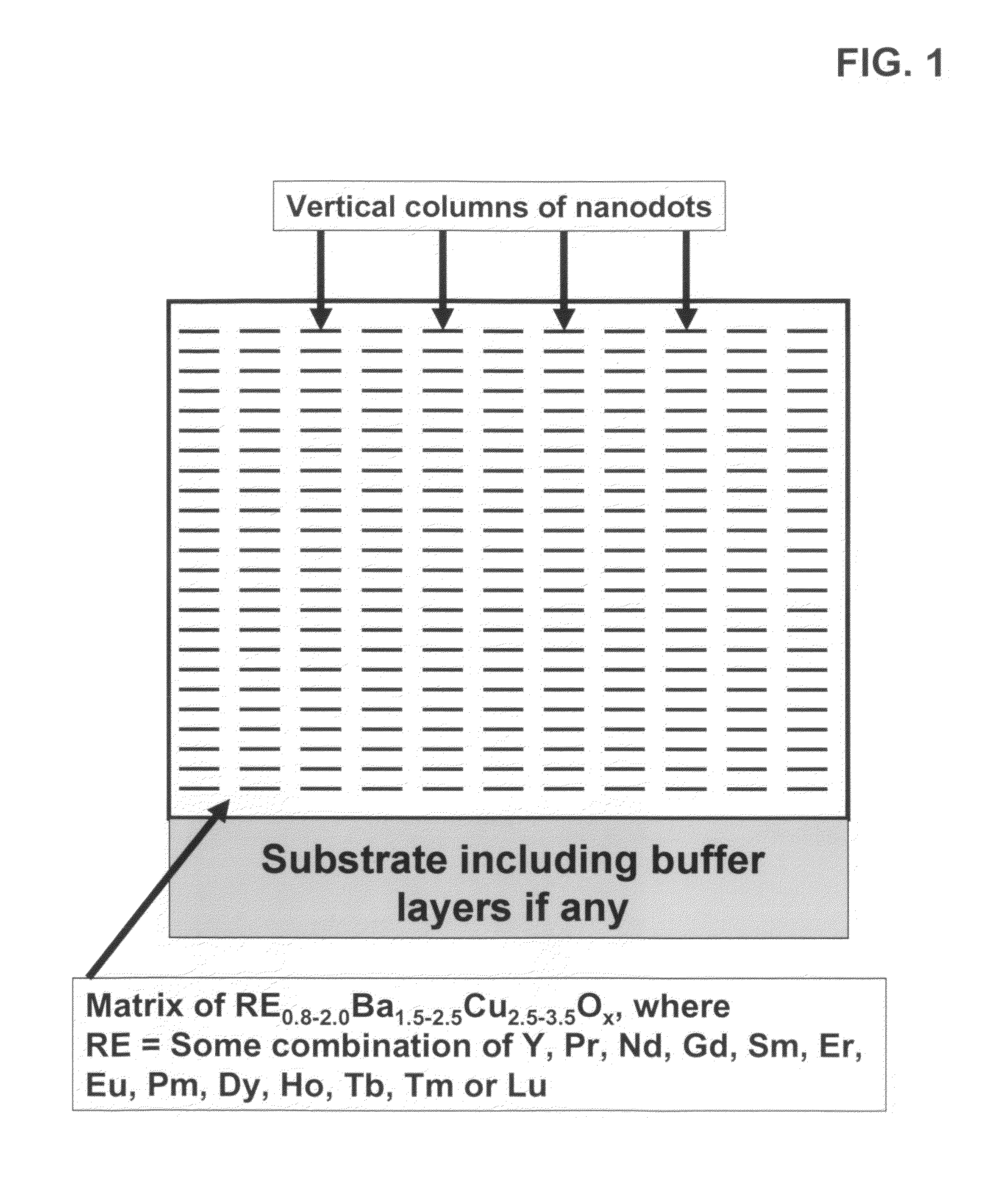
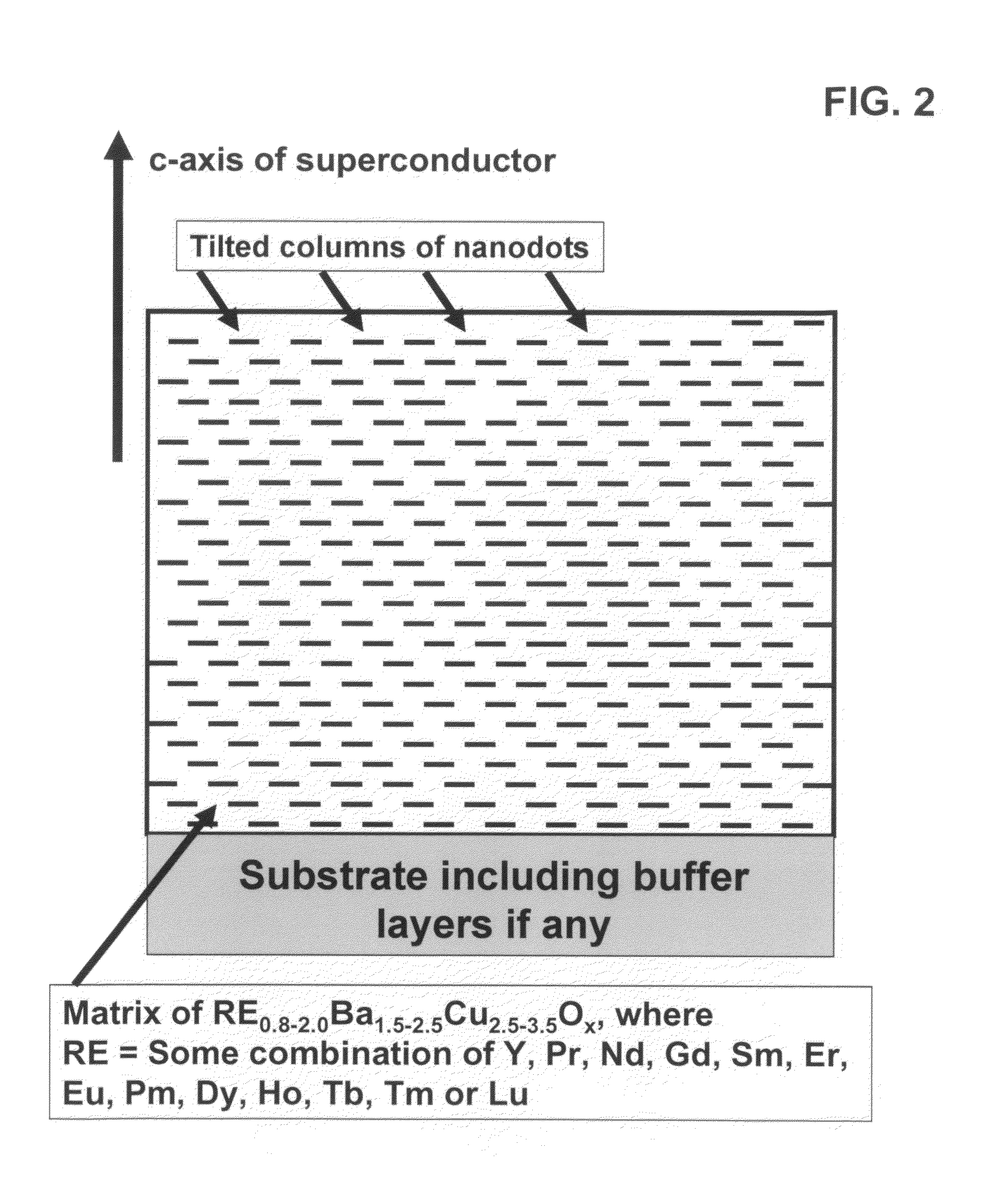
[0064]An epitaxial, composite, superconductor film is fabricated on a biaxially textured substrate IBAD with the self-assembled nanodots and / or of BZO using an in-situ deposition process such as PLD, Sputtering, e-beam co-evaporation or MOCVD deposition. Examination of as-deposited film via electron microscopy shows a columnar structure of BZO, either as columns of aligned, epitaxial nanodots of BZO or aligned nanrods of BZO. Over 80% of the columns are preferentially aligned within 60° of the c-axis of the superconductor. The critical current of superconductor film at 65K, 3 T has a minimum in Ic of over than 200 A / cm at all applied field orientations and a JE (min) of greater than 20,000 A / cm2 at 65K, 3 T at all applied field orientations.


PUM

PropertyMeasurementUnit
diameteraaaaaaaaaa
diameteraaaaaaaaaa
thickaaaaaaaaaa

Abstract

Novel articles and methods to fabricate same with self-assembled nanodots and / or nanorods of a single or multicomponent material within another single or multicomponent material for use in electrical, electronic, magnetic, electromagnetic, superconducting and electrooptical devices is disclosed. Self-assembled nanodots and / or nanorods are ordered arrays wherein ordering occurs due to strain minimization during growth of the materials. A simple method to accomplish this when depositing in-situ films is also disclosed. Device applications of resulting materials are in areas of superconductivity, photovoltaics, ferroelectrics, magnetoresistance, high density storage, solid state lighting, non-volatile memory, photoluminescence, thermoelectrics and in quantum dot lasers.

Description

CROSS-REFERENCE TO RELATED APPLICATIONS[0001]This application is a continuation-in-part of U.S. patent application Ser. No. 11 / 498,120, which claimed priority to U.S. provisional patent application Ser. No. 60 / 704,264, both of which are herein incorporated by reference in entirety.STATEMENT REGARDING FEDERALLY FUNDED RESEARCH OR DEVELOPMENT[0002]This invention was made with Government support under Contract No. DE-AC05-000R22725 awarded by the United States Department of Energy. The Government has certain rights in this invention.FIELD OF THE INVENTION[0003]The invention relates to fabrication of high performance electrical, electronic, magnetic, electromagnetic, or superconducting composite device layers with ordered nanodots and nanorods of another compound and articles made therefrom.BACKGROUND OF THE INVENTION[0004]Nano-sized materials may constitute key elements for advanced functional devices due to their size sensitive electrical, optical, magnetic and chemical properties. To...

Claims


Application Information

Patent Timeline
Patent Type & Authority Applications(United States)
IPC IPC(8): H01L39/12H01B12/00H01L39/24
CPCH01L39/126H01L39/143Y10T428/26H01L43/10Y10S505/704H01L39/2448H10N60/857H10N60/203H10N60/0521H10N60/0828H10N50/85
Inventor GOYAL, AMIT
Owner GOYAL AMIT
Why Eureka
Try Eureka