Polishing compound, method for polishing surface to be polished, and process for producing semiconductor integrated circuit device

a technology of integrated circuit devices and polishing compounds, applied in other chemical processes, lapping machines, manufacturing tools, etc., can solve the problems of difficult to form copper into the shape of wirings, unevenness tends to increase, and the difference in level exceeds the depth of focus in lithography, so as to suppress the polishing of silicon dioxide and achieve high removal rate. , the effect of high removal ra

Inactive Publication Date: 2008-08-21
ASAHI GLASS CO LTD
View PDF7 Cites 29 Cited by
  • Summary
  • Abstract
  • Description
  • Claims
  • Application Information

AI Technical Summary

Benefits of technology

[0022]According to the present invention, it is possible to polish SiC at a high removal rate in a process for producing a semiconductor integrated circuit device. In addition, it is possible to suppress polishing of silicon dioxide in the insulating layer on the other hand, while polishing SiC at a high removal rate.
[0023]Further, it is possible to obtain a semiconductor integrated circuit device having planarized multiplayer structure.

Problems solved by technology

That is, as wirings are increasingly multilayered due to the miniaturization and densification in the semiconductor production processes, the degree of unevenness tends to increase in the surfaces of the individual layers, resulting in a situation where the difference in level exceeds the depth of focus in lithography.
Since the vapor pressure of copper chloride gas is low, it is difficult to form copper into the shape of wirings by Reactive Ion Etching (RIE) which has been commonly used.
Therefore, it is not desirable to use such SiNx since it is against the demand for lowering the relative dielectric constant of the entire insulating layers of an integrated circuit.
In such planarization, when CMP is carried out by actually using the polishing compound, dishing or erosion may result in copper-embedded wirings, and a flat surface may not necessarily be obtained.
If lamination is continued while flatness is not secured because of such dishing or erosion, as wirings are multilayered, the degree of unevenness tends to increase on the surfaces of the individual layers, resulting in a problem such that the difference in level exceeds the depth of focus in lithography.
However, if it is attempted to eliminate the big difference in level solely by scraping off the insulating layer in the 2nd polishing step, the amount of the insulating layer to be scraped off will become large, and the amount of the copper wiring to be scraped off at the same time will also become large.
This means a substantial weight loss of wirings and results in an increase of the resistance of wirings.
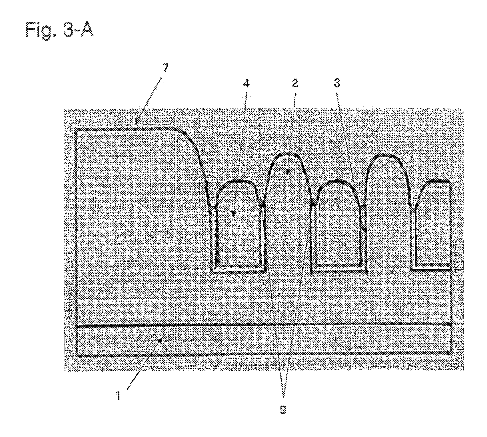
Further, as FIG. 3-B shows at number 10, it became clear that an insulating layer of the global portion close to an end of wirings becomes over-polished, and flatness will be partly deteriorated.
However, SiC is a material which has a high degree of hardness, and it is extremely difficult to form a highly planarized surface by polishing.
Further, there is a problem such that scratches are likely to be formed on the SiC layer surface by SiC fragments detached by polishing (for example, Patent Document 2).
Thus, a case study on a method of polishing a SiC layer by CMP is extremely rare.
It is disclosed that in this method, a rate of etching is low, and this indicates that mechanical polishing is major rather than chemical polishing, whereby there was a problem such that scratches are likely to be easily formed.
However, when this technique was used for polishing the SiC layer for LSI having high-density fine wirings formed, there was a problem such that scratches were likely to be easily formed.
Further, in the technique disclosed in Patent Document 3, it was difficult to use, as abrasive particles, colloidal silica which is advantageous for suppressing scratches and has a small average particle size.
Further, the technique was not sufficient also from a viewpoint of stability of the dispersion.
Therefore, the above methods could not be employed when it is desired to polish e.g. an insulating barrier layer, an etching stopper layer or an antireflection layer, made of SiC, at a high removal rate and to suppress polishing of an insulating layer made of silicon dioxide.

Method used


Image

  • Polishing compound, method for polishing surface to be polished, and process for producing semiconductor integrated circuit device
  • Polishing compound, method for polishing surface to be polished, and process for producing semiconductor integrated circuit device
  • Polishing compound, method for polishing surface to be polished, and process for producing semiconductor integrated circuit device

Examples


examples

[0093]Now, the present invention will be described in further detail with reference to Examples (Examples 1 to 16) and Comparative Examples (Examples 17 to 19).

[0094](1) Preparation of Polishing Compounds

[0095](i) Each of polishing compounds of Examples 1 and 2 was prepared as follows. To water, the inorganic acid (F) and the pH buffer (G) were added, and the basic compound (E) in a half of the amount shown in Table 1 was further added, followed by stirring for 10 minutes to obtain liquid a. Then, the removal rate-adjusting agent (B) was dissolved in the organic solvent (C) to obtain liquid b having a solid content concentration of 40 mass %.

[0096]Then, the liquid b and the aqueous dispersion of abrasive particles (A) were gradually added to the liquid a, and then, the rest of the basic compound (E) was gradually added to adjust the pH to the target level. Then, H2O2 was added, followed by stirring for 30 minutes to obtain a polishing compound. The components (A) to (G) used in resp...


PUM

PropertyMeasurementUnit
boiling pointaaaaaaaaaa
viscosityaaaaaaaaaa
boiling pointaaaaaaaaaa

Abstract

To provide a polishing compound which is capable of polishing SiC at a high removal rate, or capable of suppressing polishing of silicon dioxide in an insulating layer on the other hand, while polishing SiC at a high removal rate, in production of a semiconductor integrated circuit device, whereby it is possible to obtain a semiconductor integrated circuit device having a planarized multiplayer structure.The present polishing compound comprising abrasive particles (A), an adjusting agent of removal rate (B) which is at least one selected from the group consisting of a benzotriazole, a 1H-tetrazole, a benzene sulfonic acid, phosphoric acid or organic phosphonic acid, an organic solvent (C) having a relative permittivity of from 15 to 80, a boiling point of from 60 to 250° C. and a viscosity of from 0.5 to 60 mPa·S at 25° C., and water (D).

Description

TECHNICAL FIELD[0001]The present invention relates to a polishing technology to be used in a process for producing semiconductor integrated circuit devices. More specifically, the present invention relates to a polishing compound for chemical mechanical polishing which is suitable for polishing SiC as a constituting material of e.g. an insulation barrier layer, an etching stopper layer or an antireflection layer, and it relates to a method for polishing a surface to be polished and a method for producing a semiconductor integrated circuit device by using the polishing method.BACKGROUND ART[0002]Recently, along with the progress in the integration and functionality of semiconductor integrated circuits, there has been a demand for development of micro fabrication techniques for miniaturization and densification. Planarization techniques for interlayer insulating films and embedded wirings are important in semiconductor integrated circuit production processes, in particular, in a proce...

Claims


Application Information

Patent Timeline
Patent Type & Authority Applications(United States)
IPC IPC(8): H01L21/304C09K3/14B24B37/04
CPCB24B37/044C09G1/02H01L21/3212H01L21/31053C09K3/1463H01L21/304
Inventor TAKEMIYA, SATOSHI
Owner ASAHI GLASS CO LTD
Why Eureka
Try Eureka