Method of manufacturing semiconductor device

a semiconductor and manufacturing method technology, applied in the direction of semiconductor devices, basic electric elements, electrical appliances, etc., can solve the problems of reducing the current (isub>on/sub>), deteriorating the refreshing characteristic, increasing the junction leakage current, etc., to reduce the diffusion of impurities, improve the refresh characteristic, and reduce the contact resistance

Inactive Publication Date: 2008-10-02
ELPIDA MEMORY INC
View PDF2 Cites 33 Cited by
  • Summary
  • Abstract
  • Description
  • Claims
  • Application Information

AI Technical Summary

Benefits of technology

[0031]According to the present invention, the source and drain regions of the semiconductor device having the Fin-FET are formed by positively utilizing implantation of impurities such as phosphorus and arsenic after forming of the contact holes and oozing-out of a phosphorus from the polysilicon contact plugs, thereby reducing diffusion of impurities such as phosphorus and arsenic immediately below the gate electrodes. The GIDL is thereby reduced to improve the refresh characteristic. Also, the contact plug is formed so as to contact not only the upper surface of the convex semiconductor layer but also side surfaces (two or three surfaces), thereby achieving a reduction in contact resistance.

Problems solved by technology

In the case of increasing the impurity concentration in the channel region in a selecting transistor used in the cell array of a dynamic random access memory (DRAM), however, an adverse effect of deteriorating the refreshing characteristic occurs by increasing the intensity of an electric field in the vicinity of the source-drain junction and, thereby increasing the junction leakage current.
This technique also has a problem that a reduction in ON current (Ion) and an increase in word line capacitance are caused due to an increase in channel resistance.
It is probable that there is a difficulty in applying this technique to further miniaturization.
With a metal plug, however, there is an anxiety that an increase in leakage current occurs due to a metallic contamination on the diffusion layer to deteriorate the refreshing characteristic.
In a case where an MOS transistor having fin structure is used as a selecting transistor (NMOS), if donor impurities such as phosphorus and arsenic are diffused to a position immediately below the gate electrode, there is an anxiety that the gate-induced dielectric leakage current (GIDL) is increased because the effective gate length is reduced and the area of contact between the gate electrode and a channel portion is increased relative to that in the planar structure.
However, this method has an adverse effect of increasing the resistance of the contact plug and reducing the ON current of the transistor.
In a case where Fin-FETs are used in a cell array, there is an anxiety that the GIDL is increased relative to that in the planar structure because the area of contact between the source and drain regions and the gate electrode is larger than that in the planar structure.

Method used


Image

  • Method of manufacturing semiconductor device
  • Method of manufacturing semiconductor device
  • Method of manufacturing semiconductor device

Examples


first exemplary embodiment

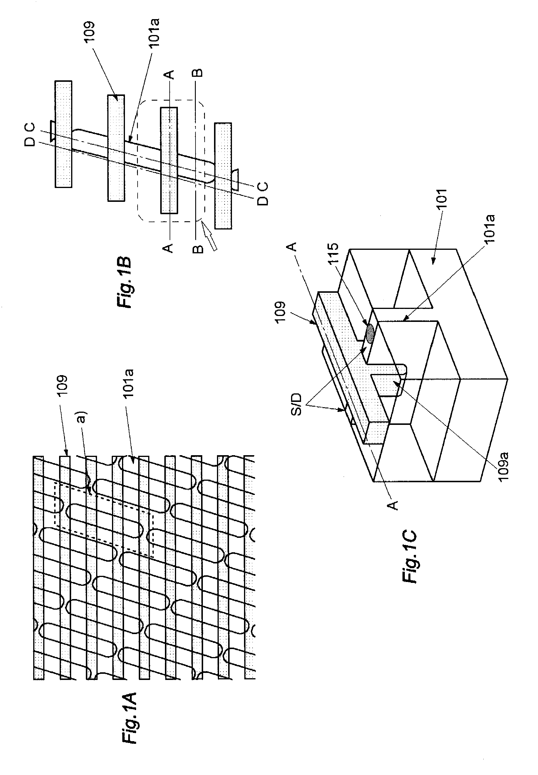
[0061]FIGS. 2 to 8, 10 to 13, and 15 are sectional views of a semiconductor device showing the process of forming a Fin-FET portion for explanation of a first exemplary embodiment of the manufacturing method in accordance with the present invention. FIGS. 2A to 8A, and 10A to 13A, and 15A show sections taken along line A-A in FIG. 1B; FIGS. 2B to 8B, 10B to 13B, and 15B, sections taken along line B-B in FIG. 1B; FIGS. 2C to 8C, 10C to 13C, and 15C, sections taken along line C-C in FIG. 1B; and FIGS. 2D to 8D, 10D to 13D, and 15D, sections taken along line D-D in FIG. 1B.

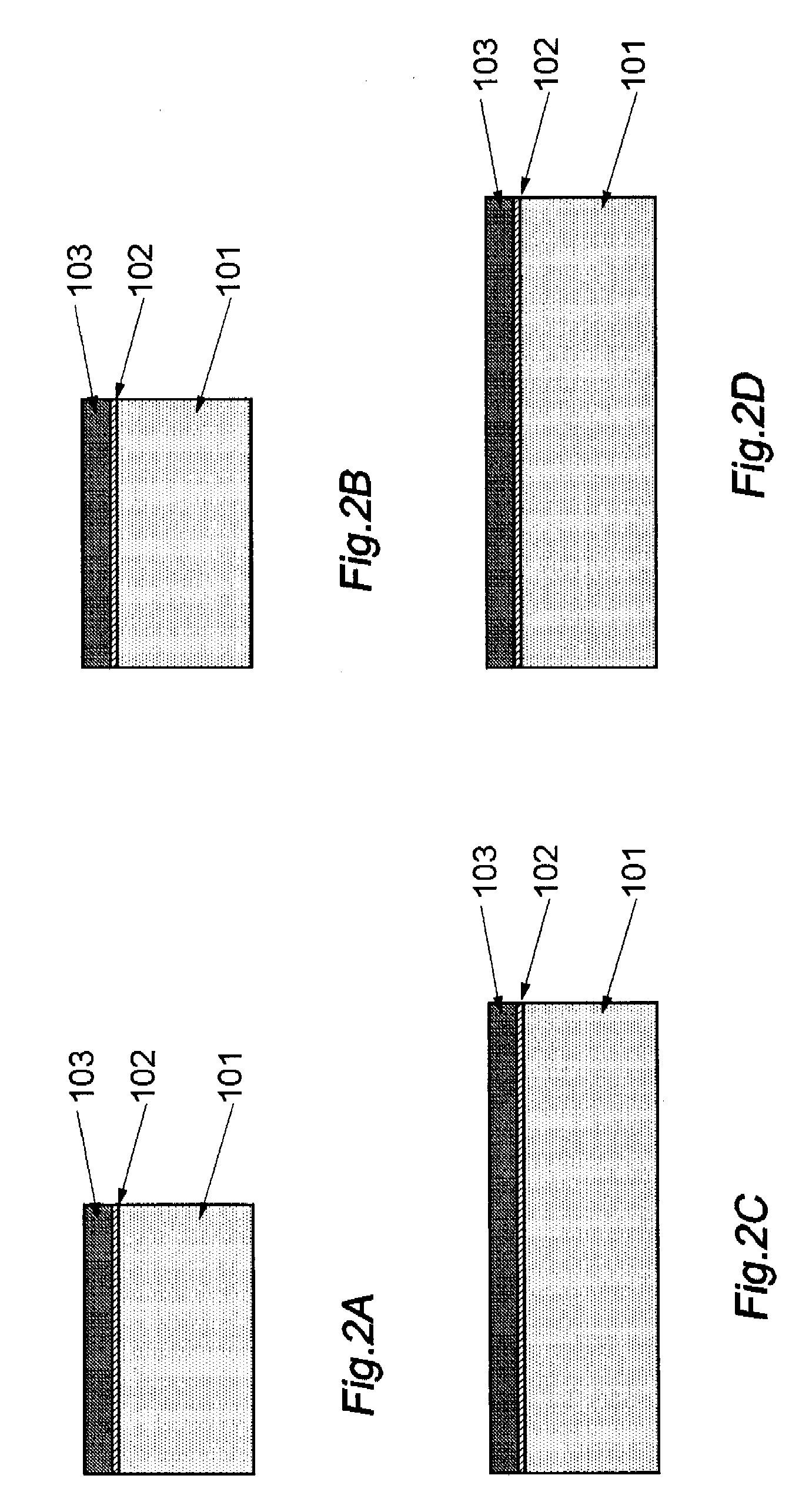
[0062]As shown in FIG. 2, pad oxide film 102 having a thickness of about 9 nm and field nitride film 103 having a thickness of about 120 nm are first formed successively on semiconductor substrate 101. This field nitride film 103 becomes a mask layer covering a diffusion layer and is also used as CMP stopper for an oxide film in which shallow trench isolation (STI) regions are embedded. Field nitride film 103 and pad...

second exemplary embodiment

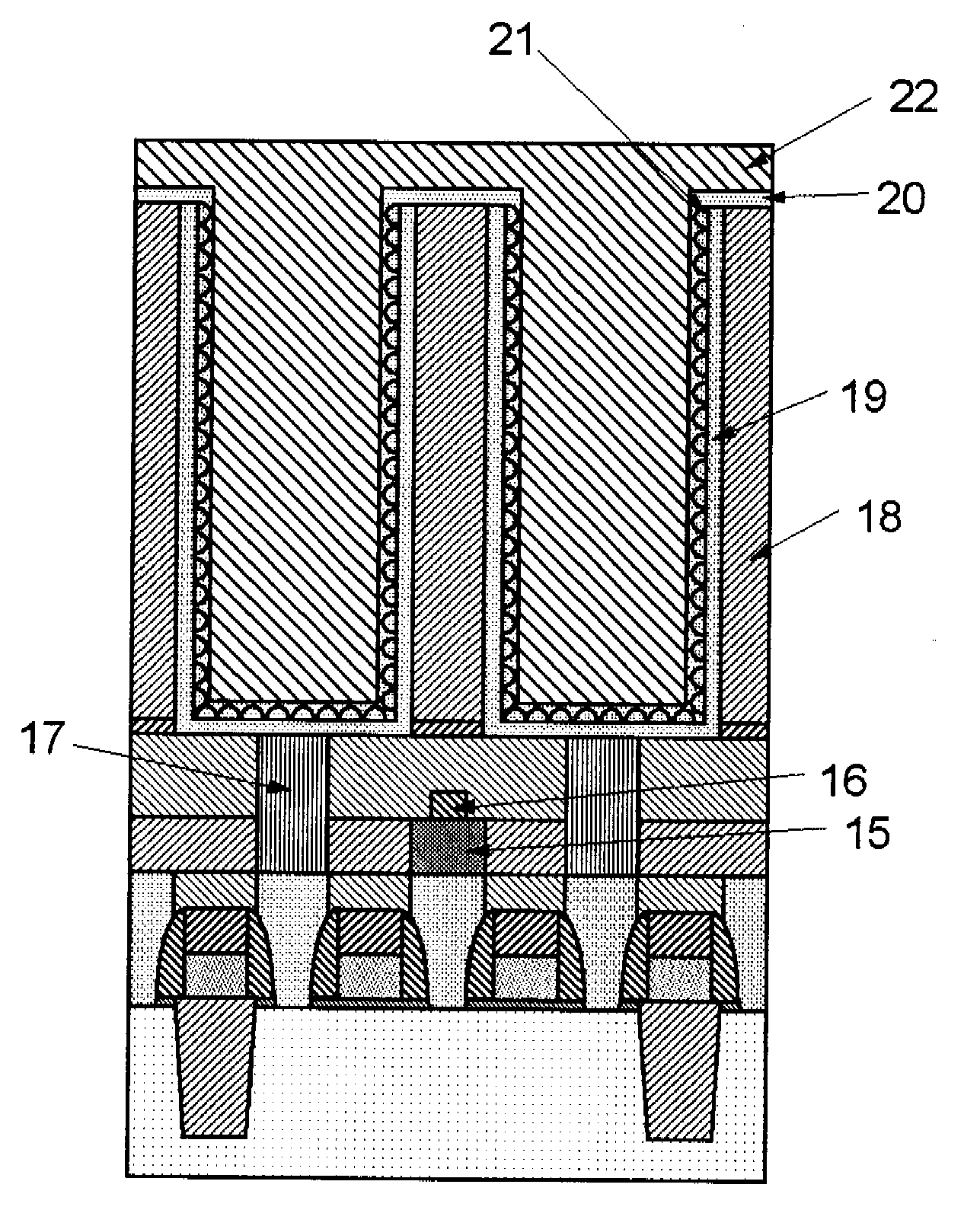
[0077]In the first exemplary embodiment, oxidation is performed after trench Si etching to form convex semiconductor layer 101b in which the length in the longitudinal direction, particularly the length of the SN portion is reduced, as shown in FIG. 17, thereby forming cell contact plug holes 13 in three directions: one upper-surface direction and two side-surface directions, and cell contact plug holes 13′ in four directions: one upper-surface direction and three side-surface directions. Thereafter, implantation of impurities, forming of plugs and solid-phase diffusion are performed, as in the first exemplary embodiment, thereby forming cell contacts 14 having side wall portions 14a and connected to bit lines between the gates and cell contacts 14′ having side wall portions 14a′ and connected to storage capacitors in the SN portion. As a result, contact surfaces 15′ can be taken in four directions for capacitor contact 14′ in the SN portion, as shown in FIG. 18B, and a further redu...


PUM


Abstract

To provide a semiconductor device using a Fin-FET and having a contact configuration such that the GIDL is reduced while limiting an increase in contact resistance, source and drain regions of the Fin-FET are formed by solid-phase diffusion positively utilizing impurity implantation after forming of contact holes 13 and oozing-out of an impurity from polysilicon contact plugs 14. Also, contact plugs 14 are extended to side surfaces of convex semiconductor layers 101a to form side wall portions 14a, thereby increasing the contact area.

Description

[0001]This application is based upon and claims the benefit of priority from Japanese patent application No. 2007-081703, filed on Mar. 27, 2007, the disclosure of which is incorporated herein in its entirety by reference.BACKGROUND OF THE INVENTION[0002]1. Field of the Invention[0003]The present invention relates to a method of manufacturing a semiconductor device and, more particularly, to a method of manufacturing a semiconductor storage device using a fin field-effect transistor (hereinafter referred to as “Fin-FET”).[0004]2. Related Art[0005]With the progress in miniaturization of semiconductor elements, the impurity concentration in the channel region has been increased for the purpose of preventing punch-through in transistors. In the case of increasing the impurity concentration in the channel region in a selecting transistor used in the cell array of a dynamic random access memory (DRAM), however, an adverse effect of deteriorating the refreshing characteristic occurs by in...

Claims


Application Information

Patent Timeline
Patent Type & Authority Applications(United States)
IPC IPC(8): H01L21/336
CPCH01L27/10876H01L27/10879H01L29/41791H01L29/66795H01L29/7851H01L2029/7858H10B12/056H10B12/053
Inventor SUGIOKA, SHIGERU
Owner ELPIDA MEMORY INC
Why Eureka
Try Eureka