
Semiconductor Device and Method of Fabricating the Same

a semiconductor and semiconductor technology, applied in the field of semiconductor devices, can solve the problems of unable to provide a substrate adapted to grow a nitride-based semiconductor having a high quality, difficulty in growing an ingan layer and an algan layer including a large amount of indium (in) or aluminum, and achieves the effects of high brightness, high capacity and large area

Inactive Publication Date: 2008-10-23
SAMSUNG ELECTRONICS CO LTD
View PDF4 Cites 59 Cited by
  • Summary
  • Abstract
  • Description
  • Claims
  • Application Information

AI Technical Summary

Benefits of technology

[0054]The semiconductor device according to the present invention exhibits high-quality, large area, high brightness, and high capacity. In addition, the layers or the light emitting structure provided in the semiconductor device of the present invention cannot be thermally or mechanically deformed or dissolved. Further, the semiconductor device according to the present invention may employ a high-performance semiconductor epitaxial layer.

Problems solved by technology

However, although various endeavors have performed for several years in various industrial fields to provide the light emitting device having the large area, high capacity, and high brightness, such endeavors have ended in a failure due to the following basic difficulties related to materials and technologies.
First, a difficulty of providing a substrate adapted to grow a nitride-based semiconductor having a high quality.
Second, a difficulty of growing an InGaN layer and an AlGaN layer including a great amount of indium (In) or aluminum (Al).
Third, a difficulty of growing a p-nitride-based semiconductor having a higher hole carrier density.
Fourth, a difficulty of forming a high-quality ohmic contact electrode (=ohmic contact layer) suitable for an n-nitride-based semiconductor and a p-nitride-based semiconductor.
However, since the nitride-based top emission type LED employing the p-ohmic electrode layer consisting of nickel-gold (Ni—Au) includes gold (Au) that reduces the light transmittance, the nitride-based top emission type LED represents a low EQE (external quantum efficiency), so the nitride-based top emission type LED is not suitable for the next-generation LED having the high capacity, large area and high brightness.
However, although the p-ohmic electrode layer fabricated through the above method can improve the light transmittance, the interfacial characteristic between the p-ohmic electrode layer and the p-nitride-based cladding layer is deteriorated, so the p-ohmic electrode layer is not suitable for the MESA-structured top emission type nitride-based LED.
However, although the p-ohmic electrode layer employing the ITO transparent layer can maximize the EQE of the LED, a great amount of heat may be generated when the nitride-based LED is operated because the p-ohmic electrode layer has a relatively high specific contact ohmic resistance value, so the above p-ohmic electrode layer is not suitable for the nitride-based LED having the large area, high capacity, and high brightness.
However, the LED disclosed in the above patent requires a complicated process to form a p-ohmic contact layer and employs gold (Au) or silver (Ag), so this LED is not suitable for the nitride-based LED having the high capacity, large area and high brightness.
In these days, many companies recognize that the MESA-structured top-emission type nitride-based LED including the transparent p-ohmic electrode layer combined with a nitride-based light emitting structure grown on a sapphire substrate may not be suitable for the next-generation LED having the high capacity, large area and high brightness because of great amount of heat generated from an active layer and various interfacial layers during the operation of a light emitting device.
However, such a MESA-structured nitride-based flip-chip LED may degrade the product yield due to complicated processes.
In addition, since the p-ohmic electrode layer including the high-reflective thin metals (Ag and Rh) is thermally unstable and represents low light reflectance at a wavelength band of 400 nm or less, so the p-ohmic electrode layer is not suitable for a (near) ultraviolet light emitting diode that emits light having a short wavelength.
However, the above vertical-structured nitride-based LED requires a p-type high reflective ohmic electrode layer having thermal stability and represents total internal reflection / absorption of light, thereby causing the low EQE and low product yield and resulting in low productivity and high costs.
In particular, although the light emitting device stacked on the silicon carbide (SiC) substrate represents superior heat dissipation, there are technical difficulties and high costs in fabrication of the SiC substrate.
In addition, Since the vertical-structured nitride-based LED exhibits the low EQE due to the high light absorption, the nitride-based LED employing the SiC substrate may not be extensively used.
However, as mentioned above, the p-side down vertical-structured nitride-based LED may significantly degrade various characteristics because the high reflective p-ohmic electrode layer causes a problem in the light emitting structure that emits light having a wavelength band of 400 nm or less.
However, as described above, there is difficulty in fabrication of the high transparent conductive p-ohmic electrode layer due to bad electric characteristics of the p-nitride-based cladding layer.
However, when the nitride-based LED having the large area, high capacity and high brightness is fabricated by using the LLO technique, the product yield of the nitride-based LED is about 50% or less, so low productivity and high costs may result.
However, the sapphire and silicon carbide substrates represent fatal problems to obtain the high-performance electronic and optoelectronic devices using the GaN-based semiconductor epitaxial stack structure.
First, according to the GaN-based semiconductor epitaxial stack structure formed on the upper portion of the sapphire substrate, high-density crystalline defects, such as dislocation and stacking fault, may occur in the GaN-based semiconductor epitaxial stack structure due to the difference of the lattice constant and thermal expansion coefficient between the GaN-based semiconductor epitaxial stack structure and the sapphire substrate, thereby degrading the reliability of the device and making it difficult to fabricate or operate the GaN-based electronic and optoelectronic devices.
In addition, since the sapphire substrate has inferior thermal conductivity, the optoelectronic devices employing the GaN-based semiconductor epitaxial stack structure formed on the upper portion of the sapphire substrate do not easily emit heat to the exterior during the operation thereof, so that the life span of the devices may be shortened and the reliability of the devices may be degraded.
In addition to the above problems, due to the electrical insulating characteristic of the sapphire substrate, vertical-structured optoelectronic devices, which have been regarded as ideal optoelectronic devices, may not be achieved.
For this reason, the MESA-structured optoelectronic devices causing the high cost and low performance must be fabricated by performing the dry etching and photolithography processes.
Although the SiC substrate is advantageous than the sapphire substrate having the electrical insulating property, the SiC substrate also represents several technical and economical disadvantages.
In particular, high costs may be incurred to fabricate single-crystalline silicon carbide, which is necessary to realize the electronic and optoelectronic devices employing the high-performance GaN-based semiconductor.
In addition, since light generated from the active layer of the LED is mostly absorbed in the SiC substrate, the SiC substrate is not suitable for the next-generation LED having high efficiency.
However, the above-described methods and technologies used for the III-nitride-based epitaxial growth substrate represent the technical difficulty, high cost, low quality, and low product yield, so the future prospect of the high-performance electronic and optoelectronic devices employing the nitride-based semiconductor epitaxial stack structure is unclear.

Method used


Image

  • Semiconductor Device and Method of Fabricating the Same
  • Semiconductor Device and Method of Fabricating the Same
  • Semiconductor Device and Method of Fabricating the Same

Examples


first embodiment

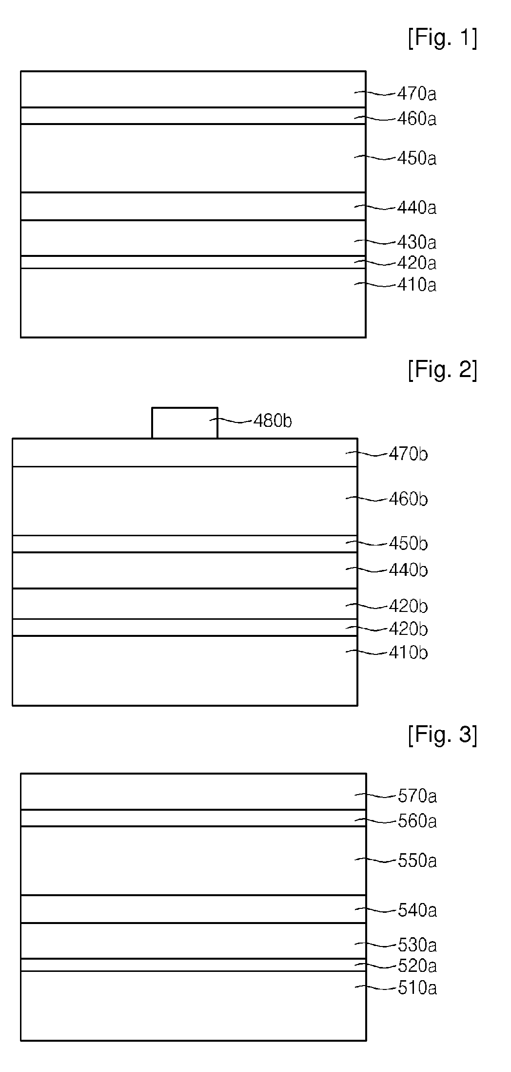
[0105]FIGS. 1 and 2 are sectional views showing p-down vertical-structured nitride-based light emitting devices fabricated by using a first tunnel junction layer introduced into an upper portion of an undoped nitride-based layer serving as a buffering layer according to the present invention.

[0106]As shown in FIG. 1, in order to fabricate a nitride-based light emitting device having the large area, high capacity and high brightness according to the present invention, a nucleation layer 420a including amorphous GaN or AlN formed at the temperature of 600° C. or below is deposited on a sapphire substrate 410a, which is an insulating growth substrate, at a thickness of 100 nm or less. Then, after forming an undoped nitride-based layer 430a serving as a buffer layer and having a thickness of 3 nm or less, a high-quality first tunnel junction layer 440a is formed on the undoped nitride-based layer 430a. After that, an n-type nitride-based thin cladding layer 450a, a multi-quantum well ni...

second embodiment

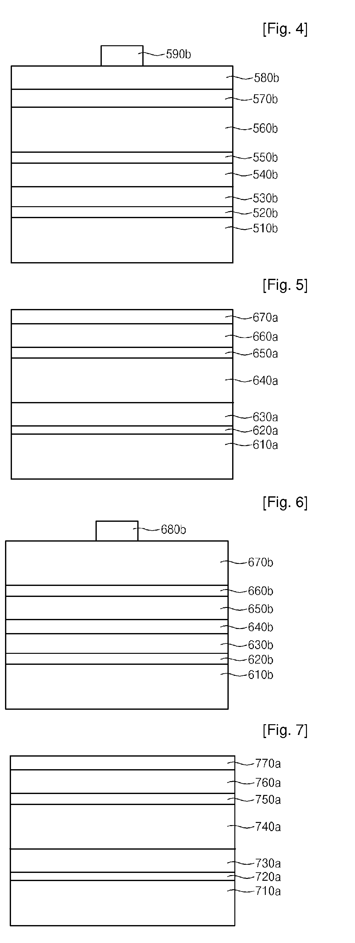
[0122]FIGS. 3 and 4 are sectional views showing p-down vertical-structured nitride-based light emitting devices fabricated by using a first tunnel junction layer introduced into an upper portion of an undoped nitride-based layer serving as a buffering layer according to the present invention.

[0123]As shown in FIGS. 3 and 4, the nitride-based light emitting structure stacked on the insulating growth substrate and the p-down vertical-structured nitride-based light emitting device are substantially identical to those of the first embodiment, except for an n-type ohmic current spreading layer 580b, which is a high transparent conductive thin film layer formed on the first tunnel junction layer 570b.

[0124]Preferably, the high transparent conductive thin film layer formed on the first tunnel junction layer 570b, that is, the n-type ohmic current spreading layer 580b includes transparent conducive oxide (TCO) or transitional metal-based transparent conductive nitride (TCN). Here, TCO is t...

third embodiment

[0130]FIGS. 5 and 6 are sectional views showing p-down vertical-structured nitride-based light emitting devices fabricated by using a second tunnel junction layer introduced into an upper portion of a p-type nitride-based cladding layer according to the present invention.

[0131]As shown in FIG. 5, in order to fabricate a nitride-based light emitting device having the large area, high capacity and high brightness according to the present invention, a nucleation layer 620a including amorphous GaN or AlN formed at the temperature of 600° C. or below is deposited on a sapphire substrate 610a, which is an insulating growth substrate, at a thickness of 100 nm or less. Then, after forming an undoped nitride-based layer 630a serving as a buffer layer and having a thickness of 3 nm or less, an n-type nitride-based thin cladding layer 640a, a multi-quantum well nitride-based active layer 650a, and a p-type nitride-based cladding layer 660a are sequentially formed on the undoped nitride-based l...


PUM


Abstract

Disclosed is a semiconductor device. The semiconductor device includes a first type nitride-based cladding layer formed on a growth substrate having an insulating property, a multi quantum well nitride-based active layer formed on the first type nitride-based cladding layer and a second type nitride-based cladding layer, which is different from the first type nitride-based cladding layer and is formed on the multi quantum well nitride-based active layer. A tunnel junction layer is formed between the undoped buffering nitride-based layer and the first type nitride-based cladding layer or / and formed on the second type nitride-based cladding layer.

Description

TECHNICAL FIELD[0001]The present invention relates to a semiconductor device. More particularly, the present invention relates to a semiconductor device having high brightness and a method of fabricating the same.BACKGROUND ART[0002]Nitride-based semiconductors are mainly used for optical semiconductor devices, such as light emitting diodes or laser diodes. III-nitride-based semiconductors are direct-type compound semiconductor materials having widest band gaps used in optical semiconductor fields. Such III-nitride-based semiconductors are used to fabricate high efficient light emitting devices capable of emitting light having wide wavelength bands in a range between a yellow band and an ultraviolet band. However, although various endeavors have performed for several years in various industrial fields to provide the light emitting device having the large area, high capacity, and high brightness, such endeavors have ended in a failure due to the following basic difficulties related t...

Claims


Application Information

Patent Timeline
IPC IPC(8): H01L31/20H01L29/12H01L33/06H01L33/12H01L33/14H01L33/32H01L33/42
CPCH01L33/04H01L33/06H01L33/12H01L33/22H01L33/405
Inventor SEONG, TAE-YEON
Owner SAMSUNG ELECTRONICS CO LTD
Learn More