

Silicon-containing film, forming material, making method, and semiconductor device
- Summary
- Abstract
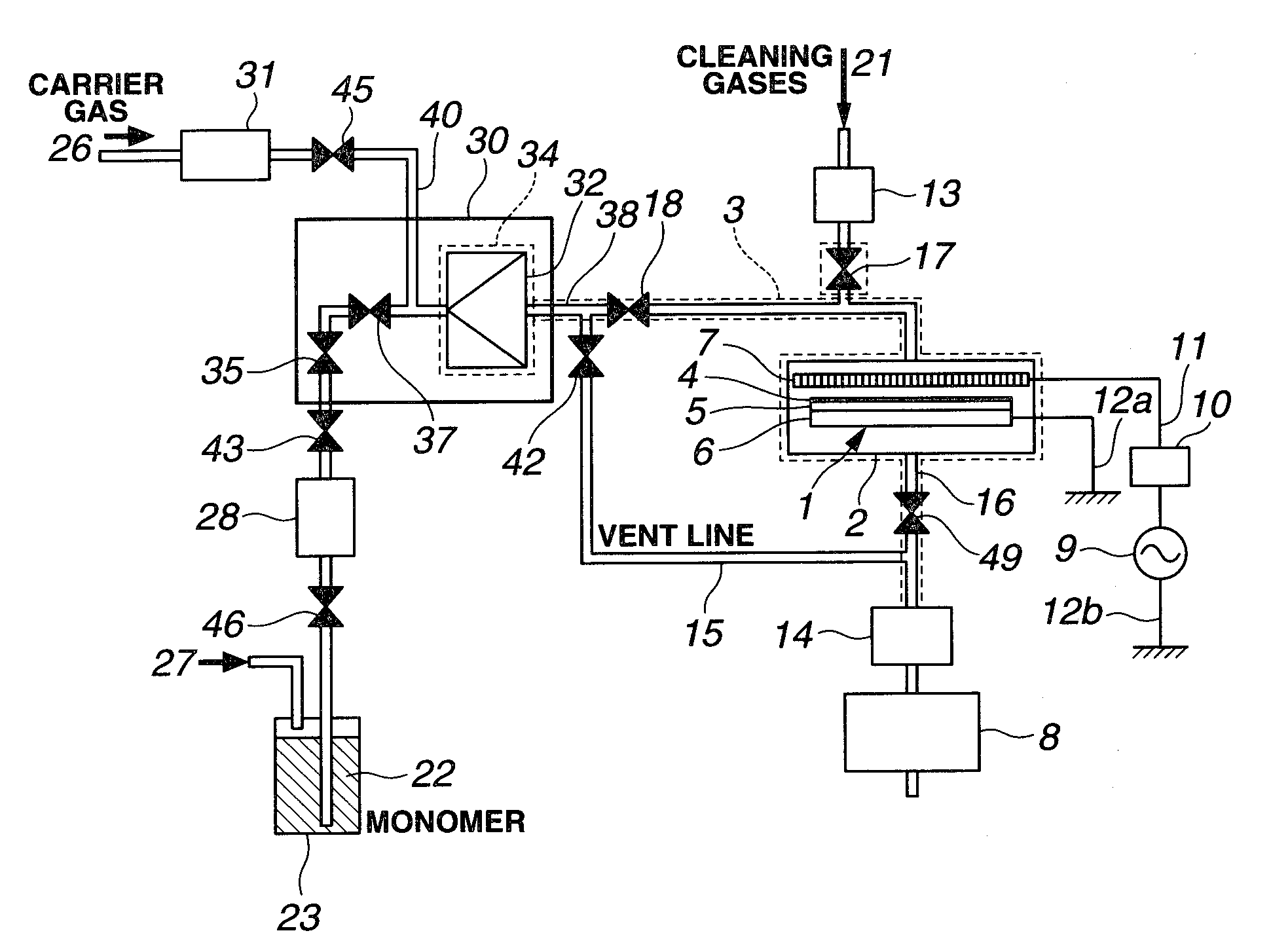
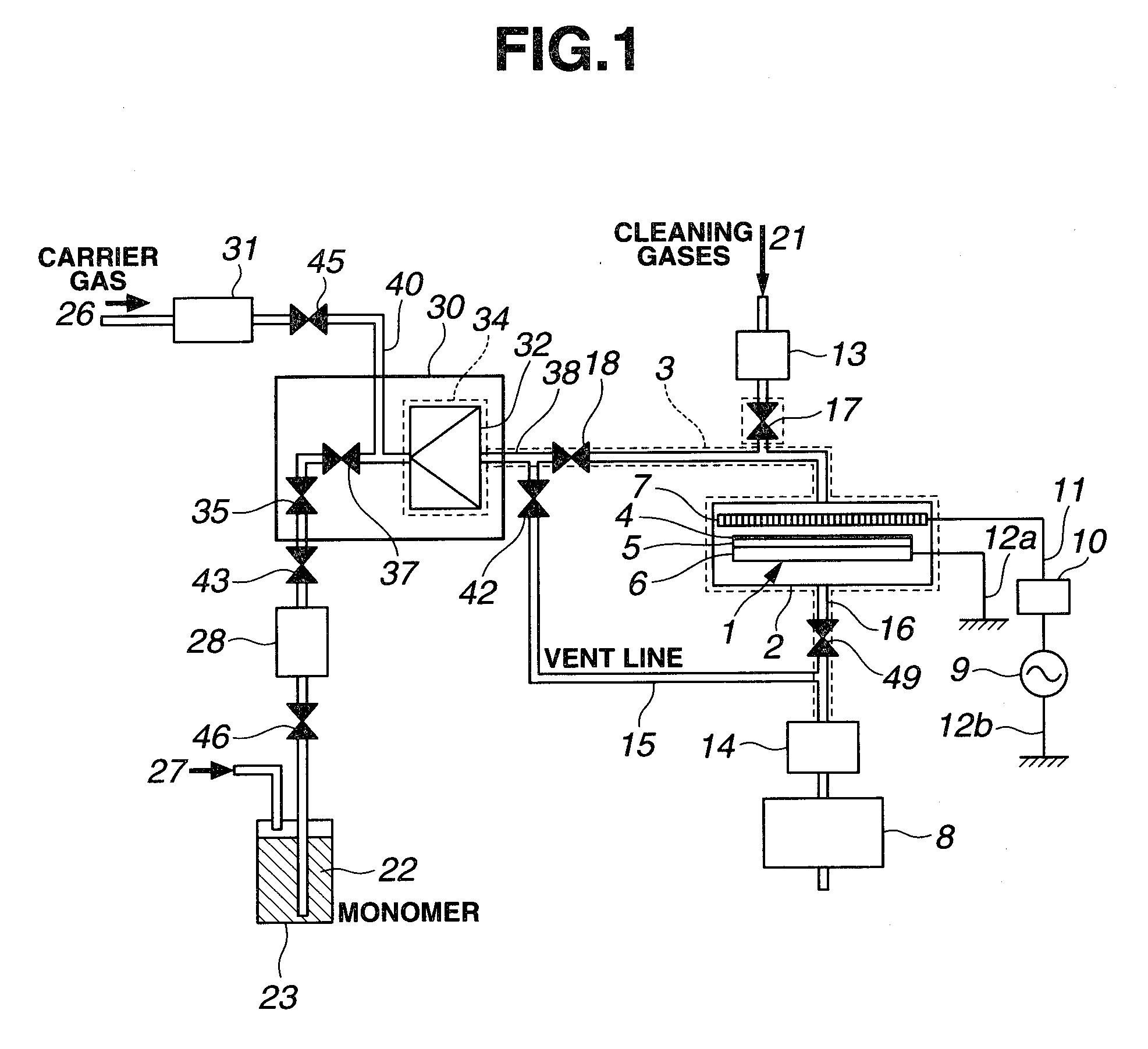
- Description
- Claims
- Application Information
AI Technical Summary
Benefits of technology
Problems solved by technology
Method used
Image

Examples
synthesis example 1
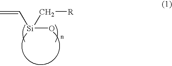
Synthesis of Propylvinyldimethoxysilane
[0080]A Grignard reagent which had been prepared from n-propyl chloride and metallic magnesium in tetrahydrofuran (THF) solvent was added dropwise to a THF solution of vinyltrimethoxysilane. Following the dropwise addition, the reaction mixture was ripened under reflux for 2 hours. Hexane was added to the reaction solution, from which the salt of Grignard reagent was removed by filtration. The end compound was collected by vacuum distillation.
synthesis example 2
Synthesis of iso-butylvinyldimethoxysilane
[0081]The end compound was obtained by the same synthesis procedure as in Synthesis Example 1 aside from using iso-butyl chloride instead of n-propyl chloride.
synthesis example 3
Synthesis of 4P4V
[0082]To a THF solution of 50 g propylvinyldimethoxysilane, obtained in Synthesis Example 1, 10 g of a 10% NaOH aqueous solution was added dropwise. The reaction mixture was ripened under reflux for 4 hours. The reaction solution was combined with ethyl acetate, and washed and neutralized with aqueous hydrochloric acid. The end compound was collected by vacuum distillation. Boiling point 75° C. / 8.5 kPa, yield 80%.
PUM
| Property | Measurement | Unit |
|---|---|---|
| Fraction | aaaaa | aaaaa |
| Fraction | aaaaa | aaaaa |
| Power | aaaaa | aaaaa |
Abstract
Description
Claims
Application Information