

Semiconductor substrate, semiconductor device and manufacturing method thereof
- Summary
- Abstract
- Description
- Claims
- Application Information
AI Technical Summary
Benefits of technology
Problems solved by technology
Method used
Image

Examples
embodiment mode 1
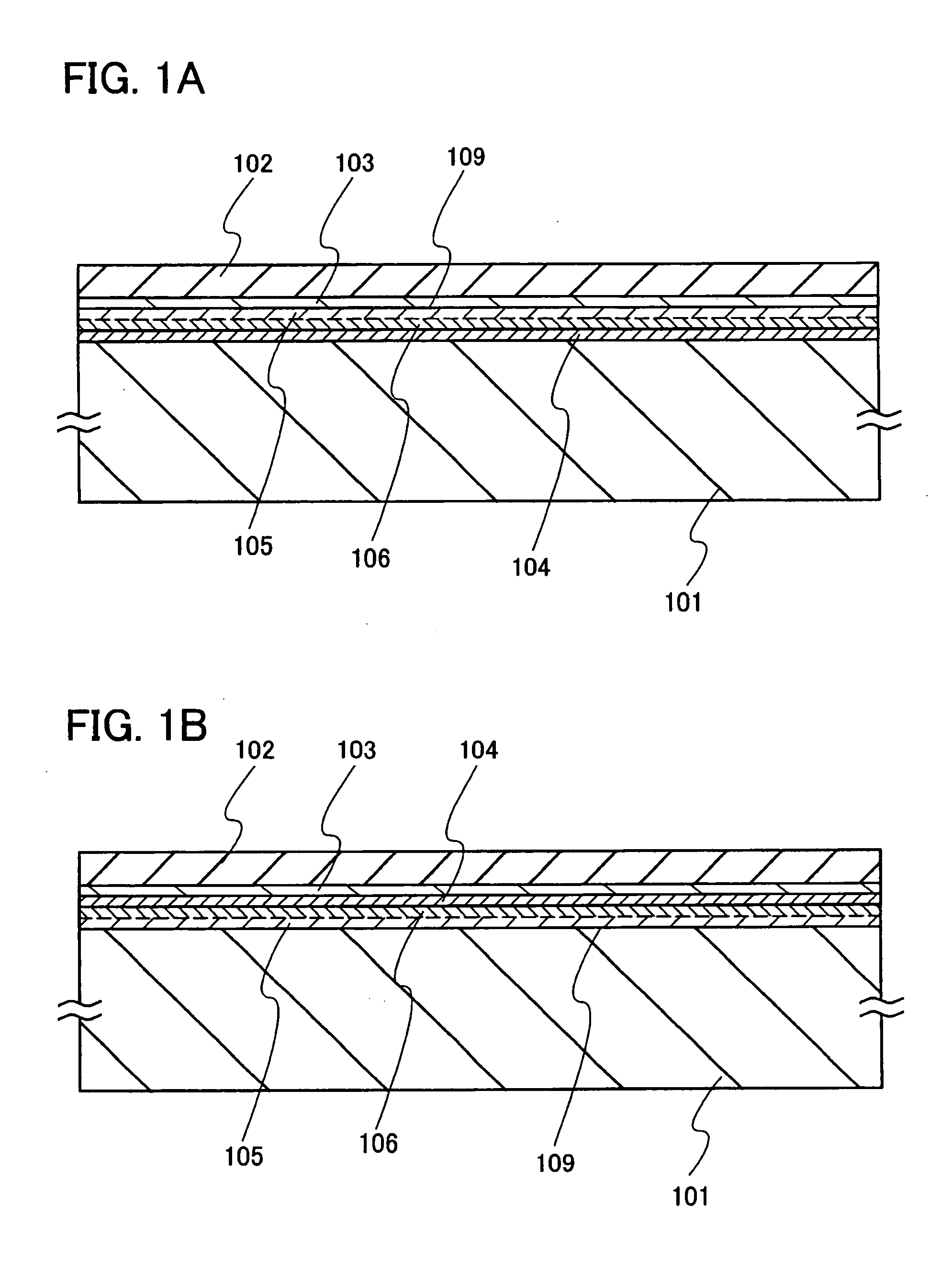
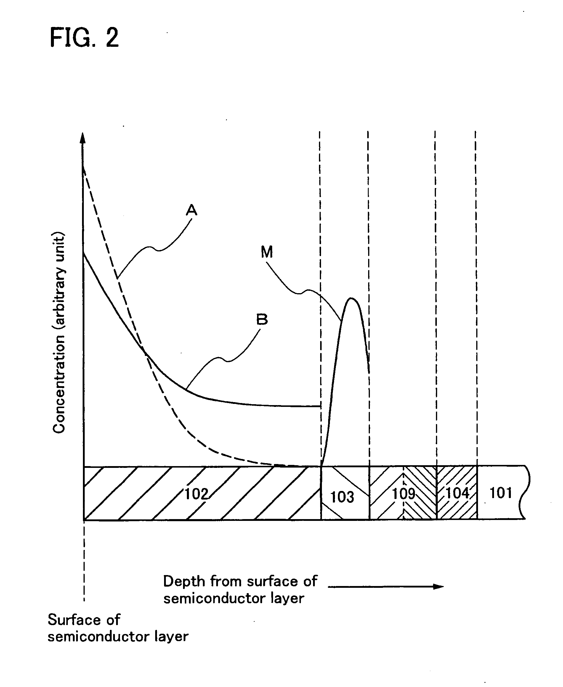
[0037]FIGS. 1A and 1B each show a structure of a substrate having an SOI structure in accordance with this embodiment mode. FIG. 1A shows a structure in which a single crystal semiconductor layer 102 provided with an oxide film 103 and a blocking layer 109 and a support substrate 101 are bonded with a bonding layer 104 interposed therebetween. In FIG. 1A, the support substrate 101 is a substrate having an insulating property or an insulating surface, and a glass substrate (also referred to as a non-alkali glass substrate)is applied, which is used for electronics industry using aluminosilicate glass, aluminoborosilicate glass, and barium borosilicate glass. In other words, a glass substrate can be applied, which has a thermal expansion coefficient of 25×10−7 / ° C. to 50×10−7 / ° C. (preferably, 30×10−7 / ° C. to 40×10−7 / ° C) and a strain point of 580° C. to 680° C. (preferably, 600° C. to 680° C.). In addition, a quartz substrate, a ceramic substrate, a metal substrate of a surface which ...
embodiment mode 2
[0095]This embodiment mode exemplifies reuse of a semiconductor substrate after a single crystal semiconductor layer is separated. Since the thickness of the single crystal semiconductor layer is 1 μm or less as described in Embodiment Mode 1, if a semiconductor substrate with a thickness of 400 μm is used for example, the same semiconductor substrate is used repeatedly, so that a substrate having an SOI structure can be manufactured.
[0096]A method for reusing a semiconductor substrate that has been used in manufacture of a substrate having an SOI structure is described with reference to FIGS. 10A to 10D. FIG. 10A illustrates the semiconductor substrate 108 after a separation step of the single crystal semiconductor layer. The semiconductor substrate is provided with part of the oxide film 103, part of the bonding layer 104, part of the blocking layer 109, and part of the separation layer 110, each of which are left after separation. A surface of the separation layer 110 has depress...
embodiment mode 3
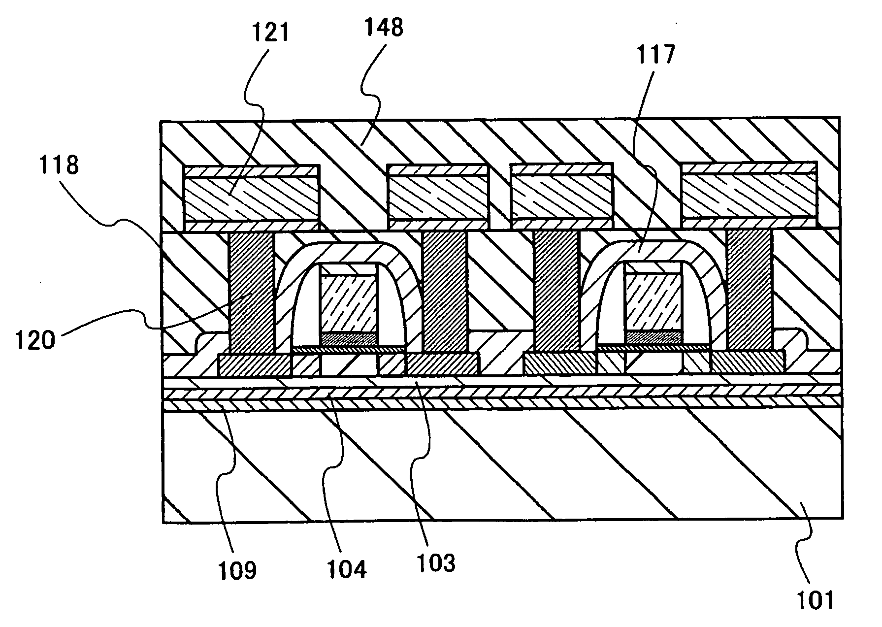
[0102]In this embodiment mode, a method for manufacturing a semiconductor device using the substrate having an SOI structure that is manufactured in Embodiment Mode 1 or 2 is described with reference FIGS. 14A to 15B. In FIG. 14A, the oxide film 103 is formed on the single crystal semiconductor layer 102 as a first insulating layer, and the blocking layer 109 as a second insulating layer and the bonding layer 104 as a third insulating layer are also formed. The single crystal semiconductor layer 102 provided with the described layers is bonded to the support substrate 101. The blocking layer 109 may be provided for the support substrate 101 side. By providing the blocking layer 109, the single crystal semiconductor layer 102 can be prevented from being contaminated by an impurity. The blocking layer 109 includes a silicon nitride layer and a silicon nitride oxide layer. Alternatively, for the blocking layer 109, an aluminum nitride layer and an aluminum nitride oxide layer may be ap...
PUM
 Abstract
Description
Claims
Application Information