Method of manufacturing silicon carbide semiconductor device

a semiconductor device and silicon carbide technology, applied in the direction of semiconductor devices, basic electric elements, electrical appliances, etc., can solve the problems of reducing contactability, deterioration of leakage characteristics, and creating asperity, so as to improve quality stability and manufacturing yield, high purity, and high quality

Active Publication Date: 2009-02-12
MITSUBISHI ELECTRIC CORP
View PDF5 Cites 38 Cited by
  • Summary
  • Abstract
  • Description
  • Claims
  • Application Information

AI Technical Summary

Benefits of technology

[0018]According to the invention, a method of manufacturing a silicon carbide semiconductor device includes a step of forming a carbon protection film of a predetermined thickness over the entire surface of a silicon carbide wafer having been ion-implanted with an impurity, using a chemical vapor deposition method that deposits a film by pyrolyzing a hydrocarbon gas. Thereby, a carbon protection film of high purity and high quality can be obtained, which prevents the silicon carbide semiconductor device from being contaminated. Moreover, since unbalanced thermal stress created in the silicon carbide wafer can also be suppressed, crystal defects associated with the thermal stress, in the silicon carbide wafer are prevented from increasing. Therefore, the method of manufacturing a silicon carbide semiconductor device can be obtained that achieves improvements in its quality stability and manufacturing yields.

Problems solved by technology

Annealing a silicon carbide wafer at such a high temperature, however, creates asperity called step bunching on the surface of the silicon carbide wafer.
The step bunching thus created becomes an obstacle in forming a gate oxide film on the silicon carbide wafer having been annealed and further becomes an obstacle in forming a gate electrode on the gate oxide film.
For example, there is a possibility of contactability reducing and of the leakage characteristic deteriorating due to asperity in the boundary surfaces between the silicon carbide wafer and the gate oxide film, or the gate oxide film and the gate electrode.
For that reason, to prevent or reduce step bunching has been a major problem for quality stability of silicon carbide semiconductor devices and for improvement in their manufacturing yields.
Accordingly, these sputtered materials scatter as contaminants, to be a source of contamination to the silicon carbide semiconductor device.
When a protection film is thus formed on only one surface of a silicon carbide wafer, unbalanced thermal stress is created in the silicon carbide wafer during an annealing treatment due to a temperature gradient produced therein and difference between the thermal expansion coefficients of the silicon carbide wafer and the protection film, which results in an increase of crystal defects in the silicon carbide wafer.
Such ingress of contaminants and increase of crystal defects are factors that contribute to unstable quality of silicon carbide semiconductor devices as well as reduction in manufacturing yields thereof.

Method used


Image

  • Method of manufacturing silicon carbide semiconductor device
  • Method of manufacturing silicon carbide semiconductor device
  • Method of manufacturing silicon carbide semiconductor device

Examples


embodiment 1

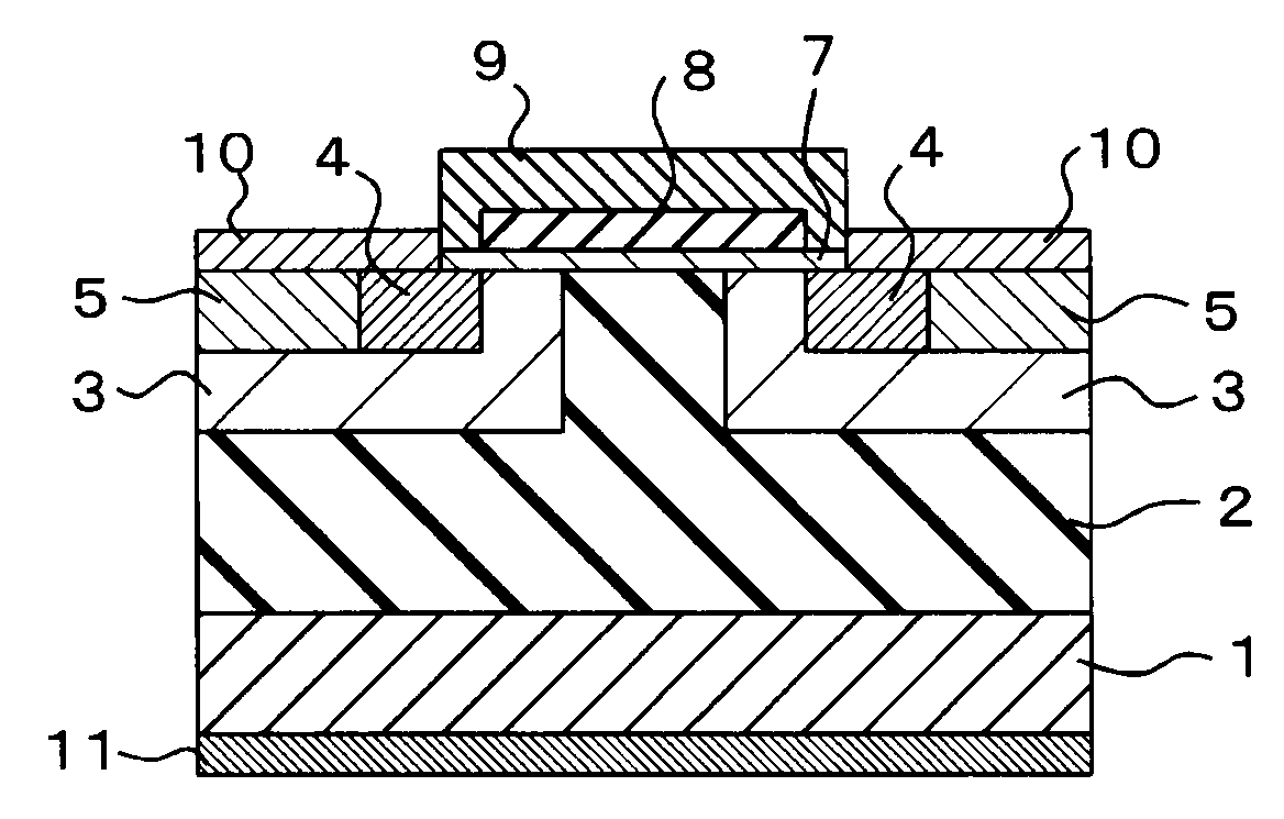
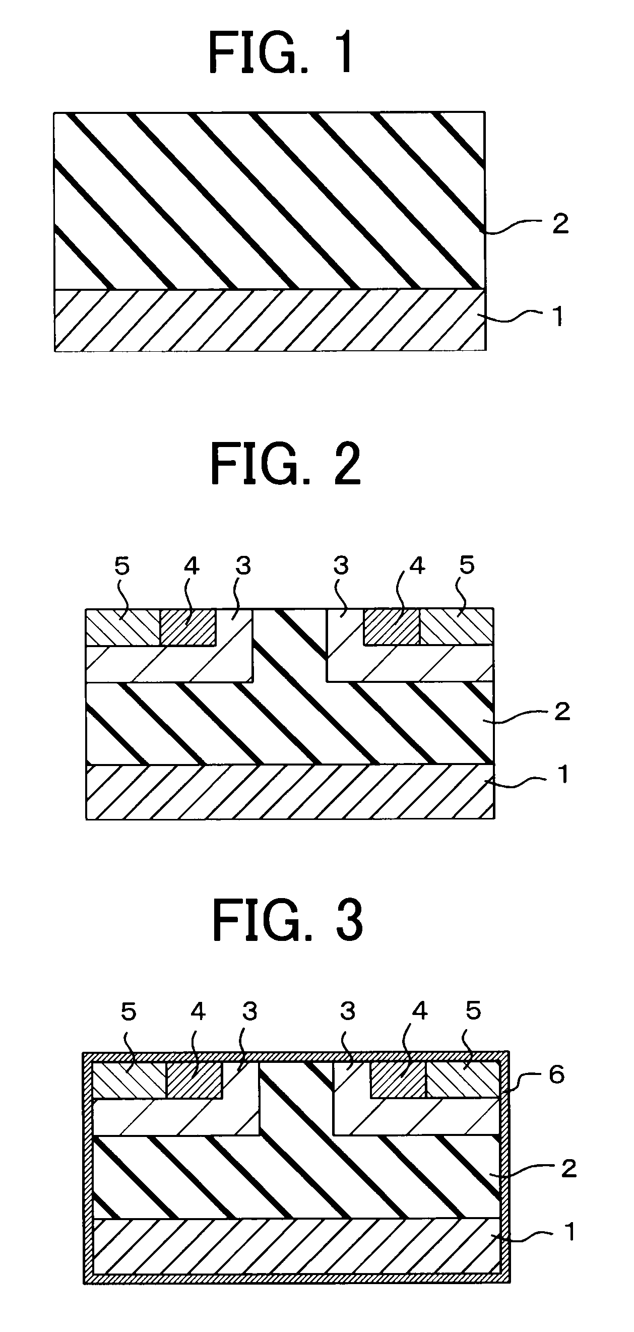
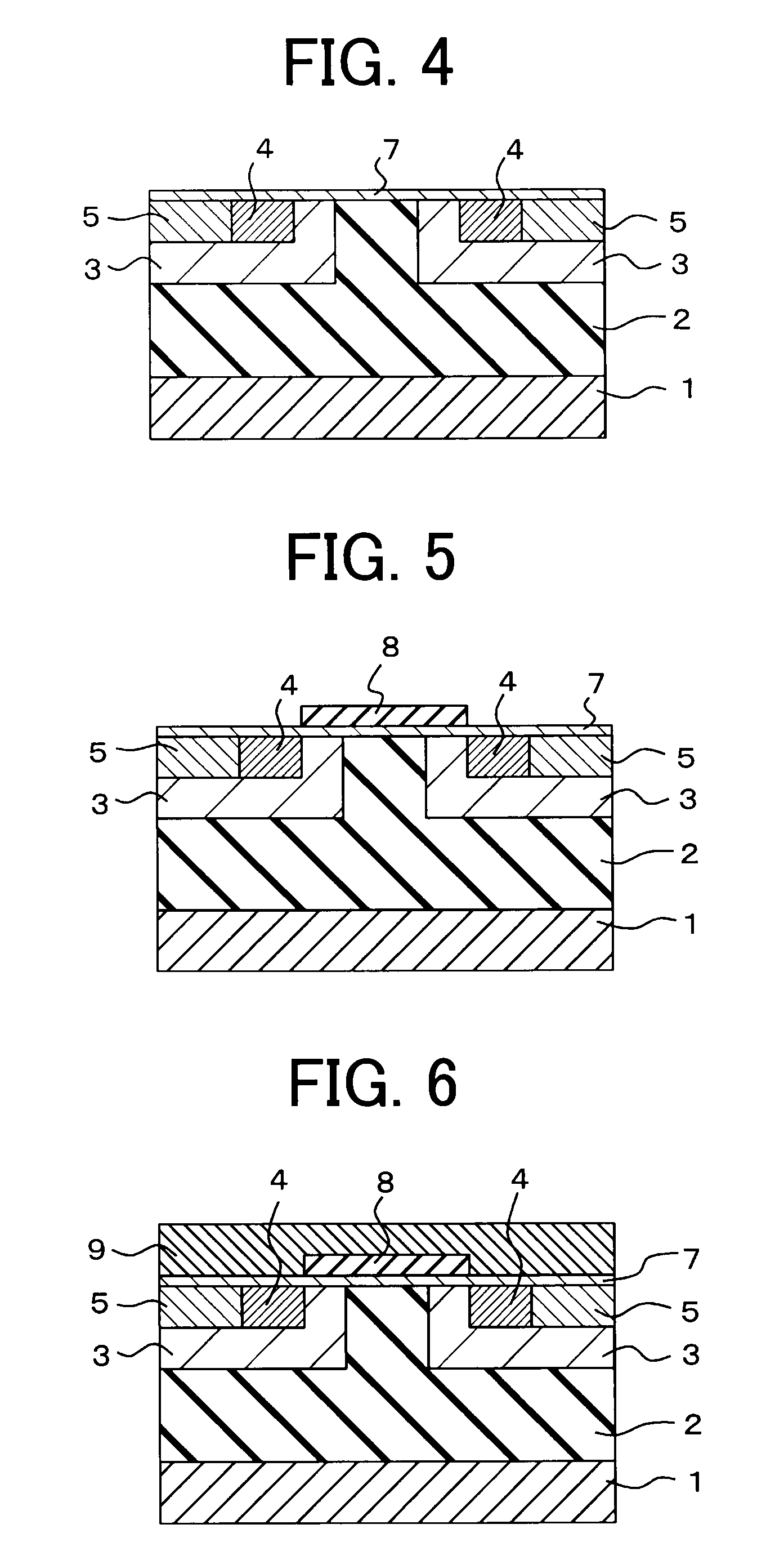
[0030]A method of manufacturing a silicon carbide semiconductor device according to Embodiment 1 of the present invention will be described. Here, a method of manufacturing a power metal-oxide semiconductor field-effect transistor (power MOSFET) is explained as an example with reference to FIGS. 1 through 8.

[0031]Firstly, an n−-type (a first conductivity-type) silicon carbide layer 2, which is made of silicon carbide, is formed on one surface of an n+-type (a first conductivity-type) semiconductor substrate 1 by epitaxial crystal growth, as shown in FIG. 1. As the semiconductor substrate 1, for example, an n+-type silicon carbide substrate is preferable. A silicon carbide wafer is made up of the semiconductor substrate 1 and the silicon carbide layer 2.

[0032]Next, a p-type (a second conductivity-type) well region 3 is formed by ion-implanting an impurity into a surface of the silicon carbide wafer using a resist as a mask for the well region. To be more specific, the impurity is ion...

embodiment 2

[0045]In Embodiment 1, the carbon protection film 6 of high quality and high purity is formed over the entire surface of a silicon carbide wafer by pyrolyzing a hydrocarbon gas such as acethylene or methane at a temperature ranging from 900° C. to 1000° C. Moreover, it is assumed in Embodiment 1 that the pyrolysis of the hydrocarbon gas and the formation of the carbon protection film 6 are performed in a CVD deposition apparatus at the same time and in the same process. In contrast, Embodiment 2 is characterized in that a CVD deposition apparatus is constituted with a gas pyrolysis furnace and a deposition furnace on the upstream and the downstream sides, respectively, with respect to a hydrocarbon gas flow, to perform pyrolysis of the hydrocarbon gas and formation of a carbon protection film 6 in separate processes in the respective furnaces. Hereinafter, a method of forming the carbon protection film 6, according to Embodiment 2 will be explained with reference to the illustration...

embodiment 3

[0053]While, in Embodiment 1 and Embodiment 2, the cases of using a hydrocarbon gas such as acethylene, methane, and propane has been explained as examples, a lower alcohol such as ethyl alcohol (C2H5OH: ethanol) and methyl alcohol (CH3OH: methanol), which is one of oxygen-containing hydrocarbons, can also be used. Here, a method of manufacturing a silicon carbide semiconductor device using ethanol or methanol will be described for a case with a power MOSFET as an example. The method of manufacturing the power MOSFET, except for a process of forming a carbon protection film, is the same as that shown in FIGS. 1 through 8 in Embodiment 1; hence the description is made with reference to FIGS. 1 through 8.

[0054]Firstly, an n−-type (a first conductivity-type) silicon carbide layer 2, which is made of silicon carbide, is formed on one surface of an n+-type (a first conductivity-type) semiconductor substrate 1 by epitaxial crystal growth, as shown in FIG. 1. As the semiconductor substrate...


PUM

PropertyMeasurementUnit
thicknessaaaaaaaaaa
thicknessaaaaaaaaaa
pressureaaaaaaaaaa

Abstract

A method of manufacturing a silicon carbide semiconductor device includes a step of ion-implanting an impurity in a surface of a silicon carbide wafer (1 and 2); a step of forming a carbon protection film (6) of a predetermined thickness over the entire surface of the silicon carbide wafer (1 and 2) having been ion-implanted with the impurity, by a chemical vapor deposition method that deposits a film by pyrolyzing a hydrocarbon gas; and a step of annealing the silicon carbide wafer (1 and 2) having been formed with the carbon protection film (6). Thereby, the carbon protection film (6) can be formed that contains extremely few contaminants, and prevents step bunching from creating on the surface of the silicon carbide wafer (1 and 2) and crystal defects created therein due to unbalanced thermal stress form increasing.

Description

BACKGROUND OF THE INVENTION[0001]1. Field of the Invention[0002]The present invention relates to methods of manufacturing a silicon carbide semiconductor device.[0003]2. Description of the Prior Art[0004]Silicon carbide (SiC) allows for manufacturing a silicon carbide semiconductor device that has a higher breakdown voltage characteristic compared to using conventional silicon (Si), and has been expected as a material for a high power semiconductor device of the next generation. In manufacturing a silicon carbide semiconductor device from such silicon carbide, in order to control its conductivity-type and conductivity, an n-type or a p-type impurity is ion-implanted into a silicon carbide wafer that consists of silicon carbide layers formed by epitaxial crystal growth on a silicon carbide substrate. After the ion implantation, in order to activate the implanted ion and remove crystal defects having been created owing to the ion implantation, the silicon carbide wafer is processed by...

Claims


Application Information

Patent Timeline
Patent Type & Authority Applications(United States)
IPC IPC(8): H01L21/265
CPCH01L21/045H01L21/046H01L21/0465H01L29/7802H01L29/1608H01L29/66068H01L21/67109
Inventor SAWADA, TAKAOWATANABE, TOMOKATSU
Owner MITSUBISHI ELECTRIC CORP
Why Eureka
Try Eureka