Soi substrates with a fine buried insulating layer

a technology of buried insulating layer and substrate, which is applied in the direction of semiconductor/solid-state device manufacturing, basic electric elements, electric apparatus, etc., can solve the problems of numerous structural defects, indirect affecting the quality of the final substrate, and difficult molecular bonding

Active Publication Date: 2009-04-30
S O I TEC SILICON ON INSULATOR THECHNOLOGIES
View PDF19 Cites 20 Cited by
  • Summary
  • Abstract
  • Description
  • Claims
  • Application Information

AI Technical Summary

Benefits of technology

[0041]Identical, similar or equivalent sections of the various figures described below have the same numerical references, making it possible to move from one figure to the next.

Problems solved by technology

However, the thinness of the insulating layer of the UTBOX substrates makes molecular bonding difficult and indirectly affects the quality of the final substrate.
In fact, with UTBOX structures, the species present at bonding interface level, such as water, hydrogen, hydrocarbons or species resulting from an implantation stage, can no longer find sufficient trapping sites within the thin oxide layer and diffuse along the bonding interface where they coalesce, giving rise to numerous structural defects.
All holes in the centre or on the edge of the wafer, whether microscopic or macroscopic in size, are killer defects, because in the absence of an active layer for the creation of electronic components, no component can be produced on this site.
However, although the various techniques currently used favour a high bonding energy at the interfaces, they do not allow very high quality semiconductor structures to be produced with thin or even ultra-thin insulating layers.

Method used


Image

  • Soi substrates with a fine buried insulating layer
  • Soi substrates with a fine buried insulating layer
  • Soi substrates with a fine buried insulating layer

Examples


first embodiment

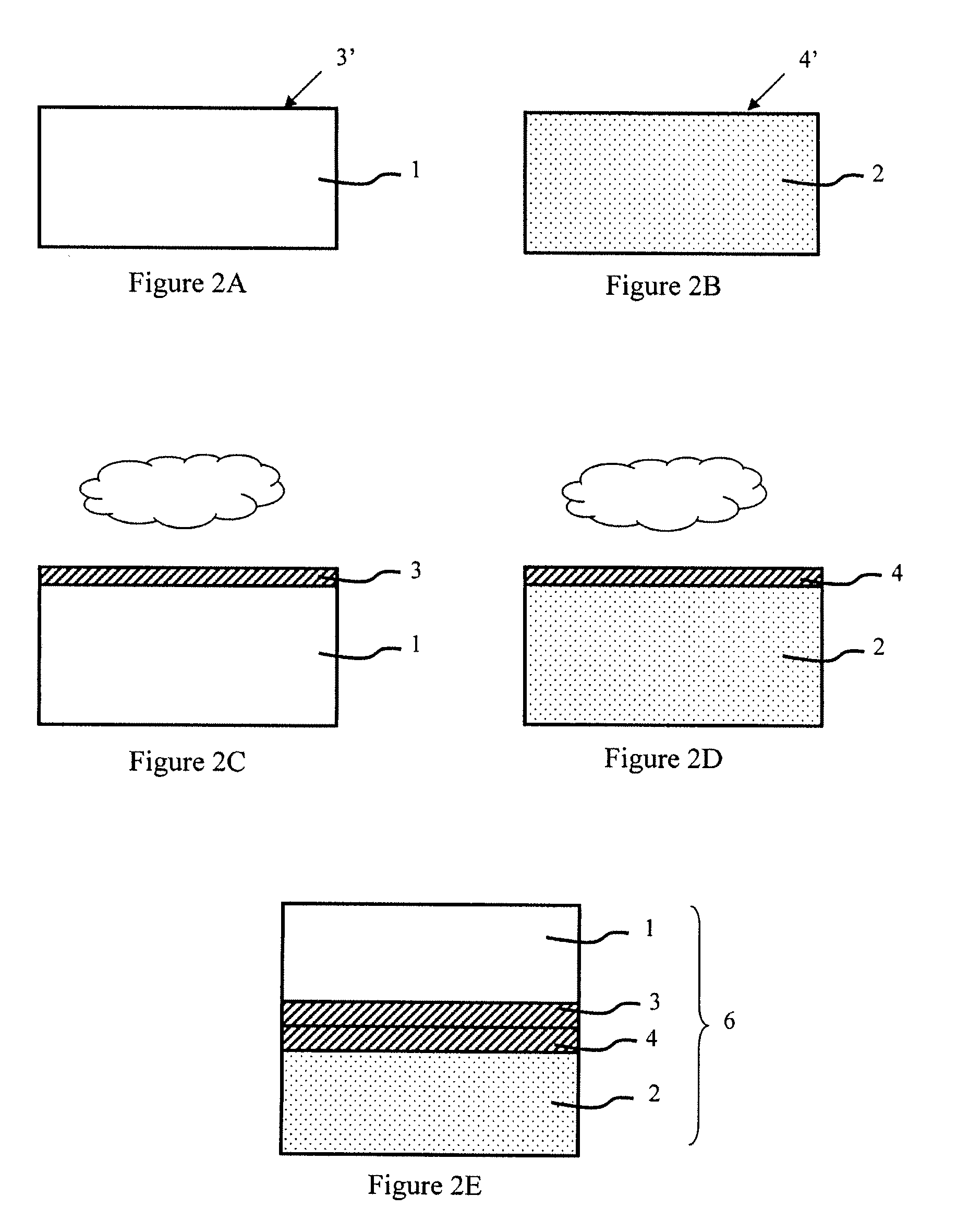
[0042]There now follows a brief description of the different successive stages in a FIG. 2A represents a first semiconductor substrate 1 with a front face 3′, while FIG. 2B represents a second substrate 2 with a front face numbered 4′. Each of the front faces of the substrates 1 and 2 undergoes plasma treatment in accordance with FIGS. 2C and 2D. An insulating layer is deliberately not created on the surface of substrates 1 and 2 before they undergo the plasma treatment according to the invention. Furthermore, a native oxide layer resulting from exposure of the substrates to the ambient air may be present on the surface of these substrates.

[0043]Hence, the front face 3′ of the first substrate 1 is subjected to treatment based on oxidizing gas, such as oxygen, water or nitrogen protoxide, in order to create an insulating layer 3 on the surface of substrate 1. If the plasma oxidizing treatment is carried out with oxygen, the pressure range is around 5 to 200 mT, the power range aroun...

second embodiment

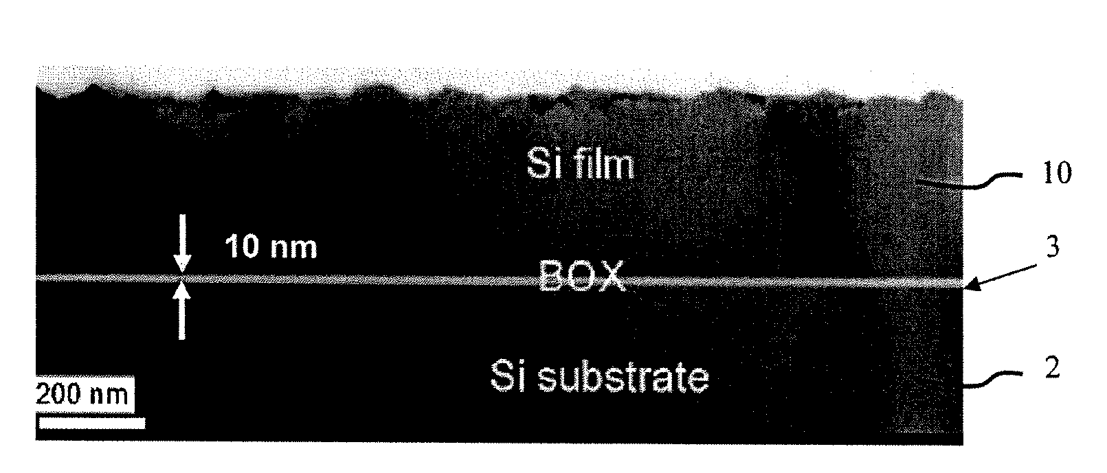
[0063]According to the example described previously, the first nitrided insulating layer 3 measuring 4 nm is brought into contact with the second insulating layer 4 of SiO2, which is 6 nm thick, so that the final structure 6 has an insulating layer with a final thickness of 10 nm. FIG. 5 shows a sectional view by transmission electron microscopy of this sort of final structure, in this case an UTBOX SOI substrate with a buried insulator 10 nm thick, obtained from the second embodiment according to the invention.

[0064]Optionally, the structure 6′ undergoes a finishing treatment involving at least one thinning and / or smoothing stage chosen from among dry or wet etching, oxidation / deoxidation, polishing and thermal treatment (such as Rapid Thermal Anneal (RTA) or long annealing in a neutral or reducing atmosphere).

third embodiment

[0065]In the third embodiment shown in FIGS. 4A to 4F, the weakened zone 5′ is made up of a porous layer obtained, for example, by a procedure known to the person skilled in the art as ELTRAN™ process. Hence, FIG. 3B shows the first substrate 1 including this porous layer 5′ defining a thin, so-called active layer 10 of a section 100 of the first substrate 1. As shown in FIG. 3C, the first substrate 1 is subjected to plasma treatment in an oxidizing atmosphere, in order to create an insulating layer 3 on the front face 3′ of the first substrate 1.

[0066]Prior to the plasma treatment stage of the first substrate 1 and before the latter is assembled with the second substrate 2, as shown in FIG. 4E, it is possible for an optional cleaning stage of surfaces 3′ and 4′ to be carried out. Bonding of the first substrate 1 and of the second substrate 2 is carried out by bringing the insulating layer 3 into close contact with the front face 4′ of the substrate 2. A thermal treatment may be app...


PUM


Abstract

A method of producing a semiconductor structure having a buried insulating layer having a thickness between 2 and 25 nm, by: forming at least one insulating layer on a surface of a first or second substrate, or both, wherein the surfaces are free from an insulator or presenting a native oxide layer resulting from exposure of the substrates to ambient conditions; assembling the first and second substrates; and thinning down the first substrate, in order to obtain the semiconductor structure. In this method, the insulating layer forming stage is a plasma activation based on an oxidizing or nitriding gas.

Description

TECHNICAL FIELD OF THE INVENTION[0001]The present invention relates to a method of producing substrates by means of the direct wafer bonding of two substrates made from materials chosen from among semiconductor materials, the final structure thereby obtained being intended, in particular, for applications in the fields of electronics, optics, photovoltaics or optoelectronics.[0002]To be more precise, this final structure is a Semiconductor On Insulator (SeOI), more particularly an SOI (Silicon On Insulator) substrate, characterized by an extremely thin (i.e., below 50 nm), buried insulator. In the event that the thin insulator should be an oxide, the substrate is said to be of an UTBOX (ultra-thin buried oxide) type. This final structure is achieved by direct wafer bonding a so-called “donor” substrate to a so-called “receiver” substrate, then thinning down the donor substrate with a view to transferring a generally thin layer of material from said donor substrate to the receiver su...

Claims


Application Information

Patent Timeline
Patent Type & Authority Applications(United States)
IPC IPC(8): H01L21/30
CPCH01L21/76254H01L21/2007H01L21/20
Inventor LANDRU, DIDIERKERDILES, SEBASTIEN
Owner S O I TEC SILICON ON INSULATOR THECHNOLOGIES
Why Eureka
Try Eureka