Fabrication of a Semiconductor Nanoparticle Embedded Insulating Film Electroluminescence Device

Inactive Publication Date: 2009-05-07
SHARP KK
View PDF9 Cites 4 Cited by
  • Summary
  • Abstract
  • Description
  • Claims
  • Application Information

AI Technical Summary

Benefits of technology

[0027]The present invention describes a high-density plasma (HDP) based process for the fabrication of an efficient EL device employing nc-Si embedded SiOxNy thin films with controlled microstructural, optical, and electrical properties. The HDP processed films show high electrical conductivity at low drive voltages, which is critical for efficient light generation by charge carrier induced optical excitations. HDP characteristics have been exploited for the creation of Si nanocrystals in a SiOxNy matrix, with PL emission in the wavelength range of 475-900 nm. The HDP deposited SiOxNy films show PL signal even in the as-deposited state, while a subsequent annealing results in significant enhancement of the PL/EL inten

Problems solved by technology

While a single layer device would obviously be more desirable, no single thin-film material has been able to provide the wide range of optical dispersion characteristics required to get the desired optical absorption, band-gap, refractive index, reflection, or transmission over a wide optical range extending from ultraviolet (UV) to far infrared (IR) frequencies.
However, the indirect band-gap makes it an inefficient material for optoelectronic devices.
Si is an indirect bandgap semiconductor with limited speed-responsivity performance, but it is still useful for detection in UV-VIS (visible)-NIR (near-IR) spectrum.
However, the indirect bandgap of Si limits the critical wavelength of Si to 1.12 μm, beyond which its absorption goes to zero, making it insensitive to two primary telecommunication wavelengths of 1.30 and 1.55 μm.
An additional issue with Si based photo-detectors is the dark current limiting the signal-to-noise ratio (SNR), and the thermal instability at operating temperatures higher than 50° C.
However, conventional PECVD and sputtering techniques have the limitations of low plasma density, inefficient power coupling to the plasma, low ion/neutral ratio, and uncontrolled bulk, and interface damage due to high ion bombardment energy.
Therefore, the oxide films formed from a conventional capacitively-coupled plasma (CCP) generated plasma may create reliability issues due to th

Method used


Image

  • Fabrication of a Semiconductor Nanoparticle Embedded Insulating Film Electroluminescence Device
  • Fabrication of a Semiconductor Nanoparticle Embedded Insulating Film Electroluminescence Device
  • Fabrication of a Semiconductor Nanoparticle Embedded Insulating Film Electroluminescence Device

Examples


Example

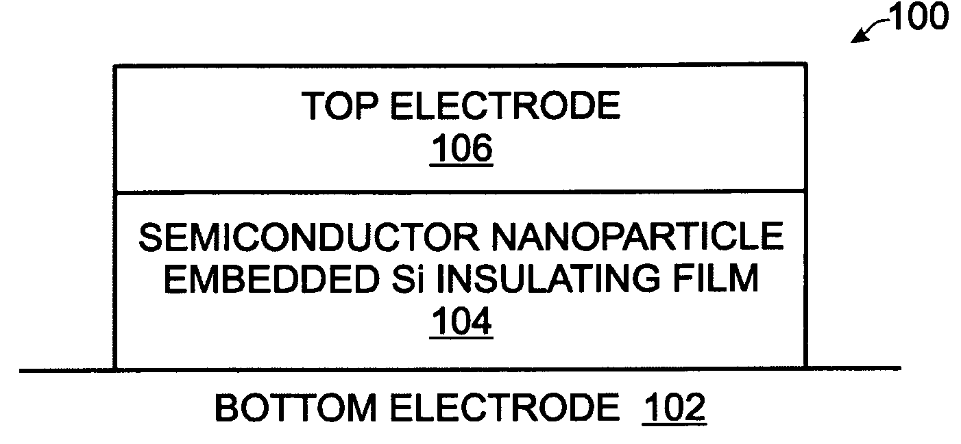
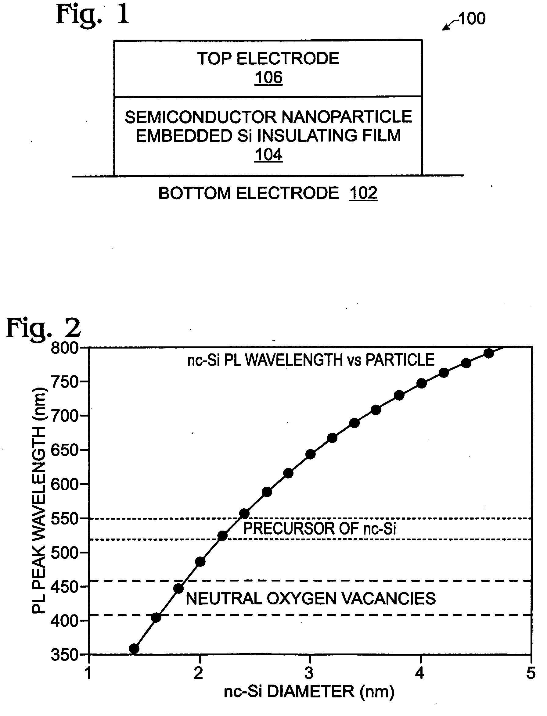
[0045]FIG. 1 is a partial cross-sectional view of an electroluminescence (EL) device with a semiconductor nanoparticle embedded Si insulating film. The EL device 100 comprises a bottom electrode 102. The bottom electrode 102 may be a doped semiconductor, metal, or polymer. A semiconductor nanoparticle embedded Si insulating film 104 overlies the bottom electrode 102. The semiconductor nanoparticle embedded Si insulating film 104 includes either the element of N or C, and has an extinction coefficient (k) in a range of 0.01-1.0, as measured at about 632 nanometers (nm). Simultaneously, the semiconductor nanoparticle embedded Si insulating film 104 has a current density (J) of greater than 1 Ampere per square centimeter (A / cm2) at an applied electric field lower than 3 MV / cm.

[0046]The semiconductor nanoparticles embedded in the Si insulating film 104 have a diameter in the range of about 1 to 10 nanometers (nm), and are made from either Si or Ge. A top electrode 106 overlies the semic...


PUM

PropertyMeasurementUnit
Temperatureaaaaaaaaaa
Pressureaaaaaaaaaa

Abstract

A method is provided for fabricating a semiconductor nanoparticle embedded Si insulating film for electroluminescence (EL) applications. The method provides a bottom electrode, and deposits a semiconductor nanoparticle embedded Si insulating film, including an element selected from a group consisting of N and C, overlying the bottom electrode. After annealing, a semiconductor nanoparticle embedded Si insulating film is formed having an extinction coefficient (k) in a range of 0.01-1.0, as measured at about 632 nanometers (nm), and a current density (J) of greater than 1 Ampere per square centimeter (A/cm2) at an applied electric field lower than 3 MV/cm. In another aspect, the annealed semiconductor nanoparticle embedded Si insulating film has an index of refraction (n) in a range of 1.8-3.0, as measured at 632 nm, with a current density of greater than 1 A/cm2 at an applied electric field lower than 3 MV/cm.

Description

RELATED APPLICATIONS[0001]This application is a Continuation-in-part of a pending patent application entitled, LIGHT EMITTING DEVICE WITH A NANOCRYSTALLINE SILICON EMBEDDED INSULATOR FILM, invented by Huang et al., Ser. No. 12 / 126,430, Attorney Docket No. SLA2270, filed May 23, 2008, which is a Continuation-in-Part of:[0002]a pending patent application entitled, SILICON OXIDE THIN-FILMS WITH EMBEDDED NANOCRYSTALLINE SILICON, invented by Pooran Joshi et al., Ser. No. 11 / 418,273, Attorney Docket No. SLA0963, filed May 4, 2006, which is a Continuation-in-Part of the following applications:[0003]ENHANCED THIN-FILM OXIDATION PROCESS, invented by Pooran Joshi et al., Ser. No. 11 / 327,612, Attorney Docket No. SLA8012, filed Jan. 6, 2006;[0004]HIGH-DENSITY PLASMA HYDROGENATION, invented by Pooran Joshi et al., Ser. No. 11 / 013,605, filed Dec. 15, 2004;[0005]DEPOSITION OXIDE WITH IMPROVED OXYGEN BONDING, invented by Pooran Joshi, Ser. No. 10 / 801,377, filed Mar. 15, 2004;[0006]HIGH-DENSITY PLAS...

Claims


Application Information

Patent Timeline
IPC IPC(8): H05B33/00H01L21/38
CPCC23C16/24H01L33/18C23C16/401C23C16/402C23C16/505C23C16/56H01L21/0214H01L21/02274H01L21/02321H01L21/0234H01L21/02532H01L21/02601H01L21/0262H01L21/31608C23C16/30
Inventor JOSHI, POORAN CHANDRAHUANG, JIANDONGVOUTSAS, APOSTOLOS T.
Owner SHARP KK
Why Eureka
Try Eureka