Carbon Nanotubes As Charge Carriers In Organic and Hybrid Solar Cells

a solar cell and carbon nanotube technology, applied in nanoinformatics, sustainable manufacturing/processing, final product manufacturing, etc., can solve the problems of low energy conversion efficiency, and low energy conversion efficiency of amorphous silicon thin-film technology, so as to improve power conversion efficiency, improve optical absorption, and enhance the efficiency of organic and inorganic/organic hybrid photovoltaic devices

Inactive Publication Date: 2009-08-20
NEW JERSEY INSTITUTE OF TECHNOLOGY
View PDF12 Cites 60 Cited by
  • Summary
  • Abstract
  • Description
  • Claims
  • Application Information

AI Technical Summary

Benefits of technology

[0017]The present disclosure also provides for methods for enhancing the efficiency of organic and inorganic / organic hybrid photovoltaic devices. In an exemplary embodiment, the present disclosure provides photovoltaic devices with enhanced power conversion efficiency by improved optical absorption and appropriate morphological rearrangement.

Problems solved by technology

Ribbon technologies, which incorporate a variation on the multi-crystalline production process, use fewer types of raw materials but also have lower energy conversion efficiency.
Thin-film technologies have several drawbacks however.
Amorphous silicon thin-film technologies use expensive silicon and have relatively low energy conversion efficiencies.
The main drawback of cadmium telluride thin-film technologies is the toxicity of cadmium.
The main disadvantages of copper indium diselenide and copper indium gallium diselenide technologies are the complexity involved in the manufacturing process, as defects easily form, and safety issues concerning the manufacturing process, which involves the extremely toxic gas hydrogen selenide.
The main drawback to this technology is the requirement of expensive tracking systems.
Concentrator photovoltaics can only use direct sunlight and therefore require a means to follow the movement of sunlight.
While silicon is very expensive, GaAs is fragile, a known carcinogen and is even more expensive than silicon.
Most existing technologies use expensive raw materials.
Some traditional solar cells incorporate glass or plastics which makes the cells heavy, potentially dangerous, and expensive to ship.
Some cells are expensive to install because they must be specially mounted or integrated with expensive tracking mechanisms.
Other technologies use dangerous materials in the manufacturing process or final product.
Also, up to 70% of the expensive silicon is wasted during some silicon solar cell manufacturing methods.
Another drawback of some traditional silicon based photovoltaics is that they are rigid.
The electronics required for traditional cells adds further complexity to using them as anything other than standalone add-ons for devices or buildings.
Lastly, existing silicon and other solar cell technologies may be reaching their limit in terms of cost to efficiency ratios.
The main drawback to OPVs is that they are much less efficient at converting light into electricity as compared to silicon based devices.
In addition, PCBM is intrinsically more expensive than C60 because it involves the derivatization of C60 by complicated synthesis routes.
The derivatization increases the overall cost of photovoltaic devices using PCBM as the electron acceptor.
However, inefficient transport of photogenerated charge carriers, like in OPVs, is a major source of efficiency loss in QD-polymer based photovoltaic devices.
However, nanotubes distributed within a polymer matrix are less efficient in separating photogenerated carriers than spherical C60 molecules that have a larger surface to volume ratio and it is difficult to disperse CNTs in a photoactive matrix.

Method used


Image

  • Carbon Nanotubes As Charge Carriers In Organic and Hybrid Solar Cells
  • Carbon Nanotubes As Charge Carriers In Organic and Hybrid Solar Cells
  • Carbon Nanotubes As Charge Carriers In Organic and Hybrid Solar Cells

Examples


Embodiment Construction

[0039]The following describes certain exemplary embodiments of the present disclosure. It should be understood that the following is intended merely to be exemplary of the disclosure.

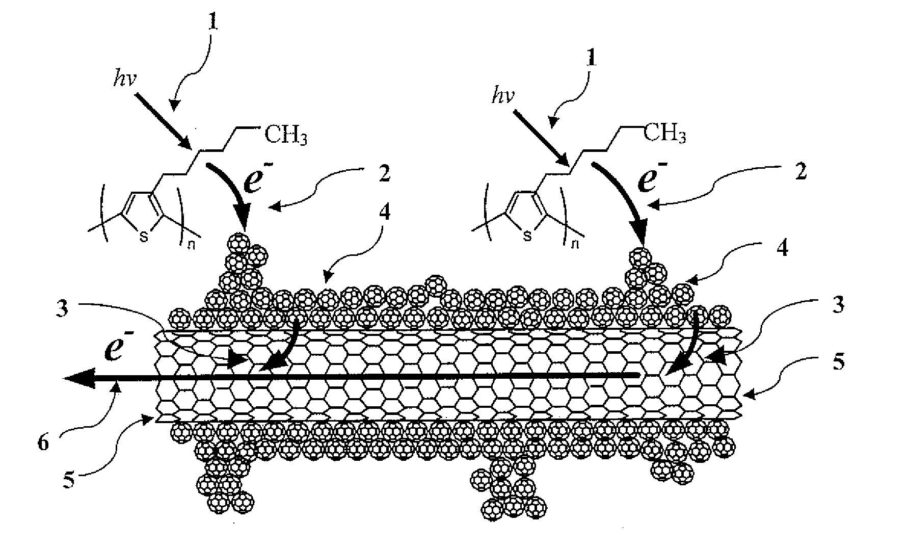
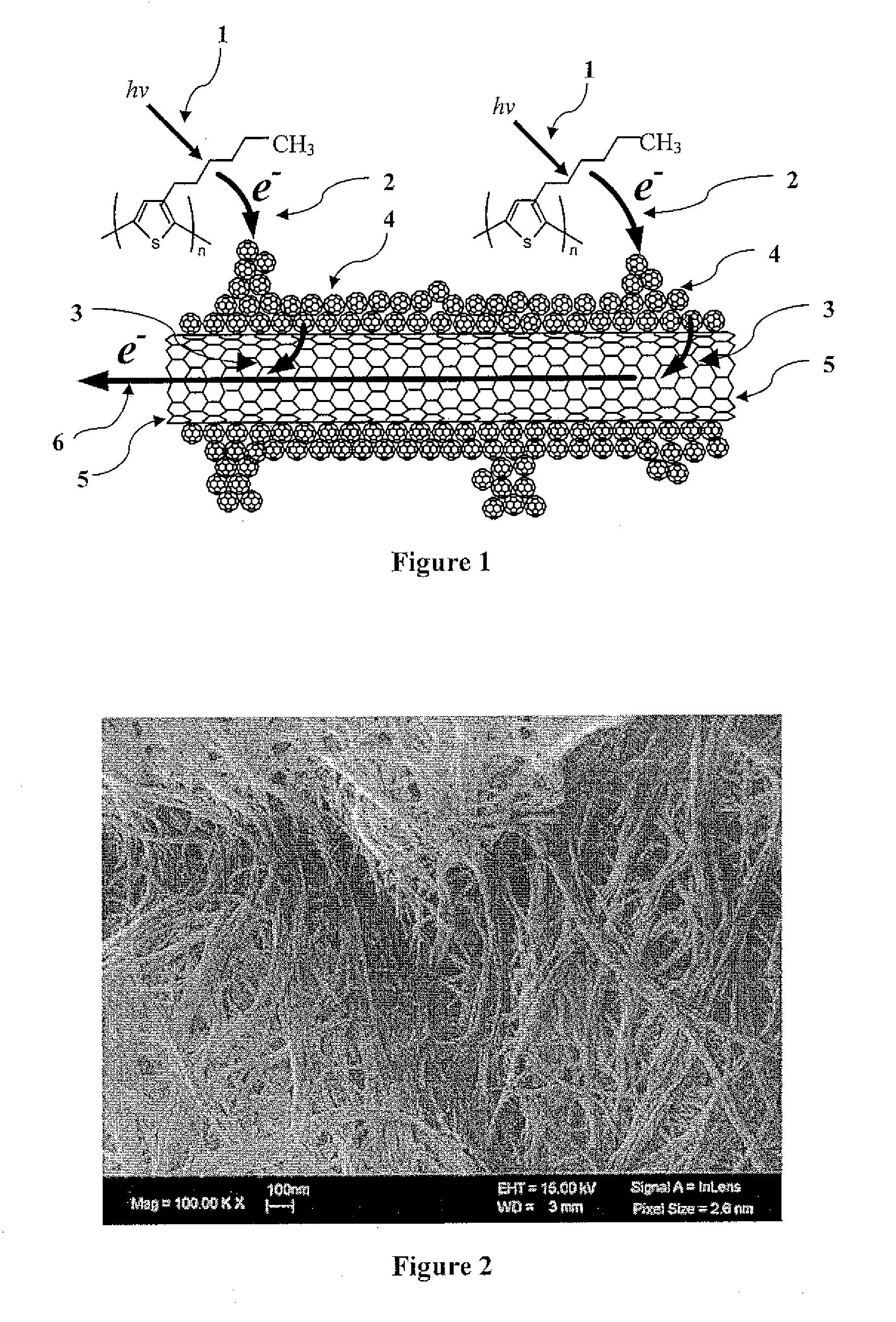
[0040]The present disclosure provides cost effective organic photovoltaic devices with increased power conversion efficiencies over previously demonstrated OPVs. The present disclosure provides polymer:fullerene C60-carbon nanotube (polymer:C60-CNT) composites adapted and / or developed for organic photovoltaic cells. The disclosed composite generally includes a polymer as the electron donator, C60 as the electron acceptor and CNTs as a means of electron transport. As FIG. 1 illustrates, under light irradiation 1, photoinduced charge separation at the polymer / C60 interface 2 is followed by electron transfer 3 from C60 4 onto bonded CNTs 5. The CNT network provides a direct path for faster electron transport towards the electrode 6.

[0041]In exemplary embodiments, C60 is employed because C60 is a stronger e...


PUM

PropertyMeasurementUnit
concentrationaaaaaaaaaa
areaaaaaaaaaaa

Abstract

Organic and organic/inorganic hybrid bulk heterojunction photovoltaic devices with improved efficiencies are disclosed. The organic photovoltaic device comprises a photoactive polymer:fullerene C60-carbon nanotube (polymer:C60-CNT) composite as a component of the active layer. Under light irradiation, photoinduced charge separation at the polymer:C60 interface is followed by electron transfer from C60 onto CNTs for efficient electron transport towards an electrode. The organic/inorganic hybrid photovoltaic device comprises quantum dots and carbon nanotubes. Power conversion efficiency enhancement methods of polymer-CNT based photovoltaics are also provided.

Description

[0001]The present invention was made at least in part with funding received from the U.S. Army Research Office under grant DAAE30-03-D-1015. The U.S. Government may have certain right in this invention.TECHNICAL FIELD[0002]The present invention generally relates to organic and organic / inorganic hybrid photovoltaic devices, e.g., solar cells. More specifically, the invention is directed to the use of carbon nanotubes as electron transporters in organic and organic / inorganic hybrid photovoltaic devices.BACKGROUND OF THE DISCLOSURE[0003]Rising energy prices, the growing dependency on foreign oil, and environmental concerns have increased public and government interest in renewable sources of electricity generation. Photovoltaic devices, also known as solar cells, generate electrical power from ambient light. The solar power market has continuously grown in popularity and the ability to create high-efficiency solar cells is a key strategy to meeting growing world energy needs. Today's p...

Claims


Application Information

Patent Timeline
Patent Type & Authority Applications(United States)
IPC IPC(8): H01L31/00B05D5/12C08K3/04
CPCB82Y10/00H01L51/0036Y02E10/549H01L51/0048H01L51/4253H01L51/0046Y02P70/50H10K85/113H10K85/211H10K85/221H10K30/30
Inventor MITRA, SOMENATHLI, CHENG
Owner NEW JERSEY INSTITUTE OF TECHNOLOGY
Why Eureka
Try Eureka