Silicon Oxide-Nitride-Carbide with Embedded Nanocrystalline Semiconductor Particles

a silicon oxide and nano-carbide technology, applied in the solar field, can solve the problems of low plasma density, low ion/neutral ratio, low power coupling to the plasma, and inefficient pecvd and sputtering techniques, and achieve enhanced plasma reaction kinetics, high-density plasma characteristics, and minimizing plasma induced bulk and interface damage.

Inactive Publication Date: 2009-09-03
SHARP KK
View PDF21 Cites 23 Cited by
  • Summary
  • Abstract
  • Description
  • Claims
  • Application Information

AI Technical Summary

Benefits of technology

[0021]The SiOxNyCz thin films are fabricated using a high-density plasma-based process characterized by high plasma concentrations, low plasma potential, and independent control of plasma energy and density, which provide unique process possibilities and control. The high-density plasma characteristics are a result of enhanced plasma reaction kinetics. The high-density plasma deposition process is dominantly controlled by the plasma characteristics rathe...

Problems solved by technology

However, the indirect band-gap makes it an inefficient material for optoelectronic devices.
However, conventional PECVD and sputtering techniques have the limitations of low plasma density, inefficient power coupling to the plasma, low ion/neutral ratio, and uncontrolled bulk, and interface damage due to high ion bombardment energy.
Therefore, the oxide films formed from a conventional capacitively-coupled plasma (CCP) generated plasma may create reliability issues due to the high bombardment energy of the impinging ionic species.
However, it is not possible to control the ion energy using radio frequency (RF) of CCP generated plasma.
Any attempt to enhance the reaction kinetics by increasing the applied power results in increased bombardment of the deposited film, which creates a poor quality films with a high defect concentration.
Additionally, the low plasma density associated w...

Method used


Image

  • Silicon Oxide-Nitride-Carbide with Embedded Nanocrystalline Semiconductor Particles
  • Silicon Oxide-Nitride-Carbide with Embedded Nanocrystalline Semiconductor Particles
  • Silicon Oxide-Nitride-Carbide with Embedded Nanocrystalline Semiconductor Particles

Examples


Embodiment Construction

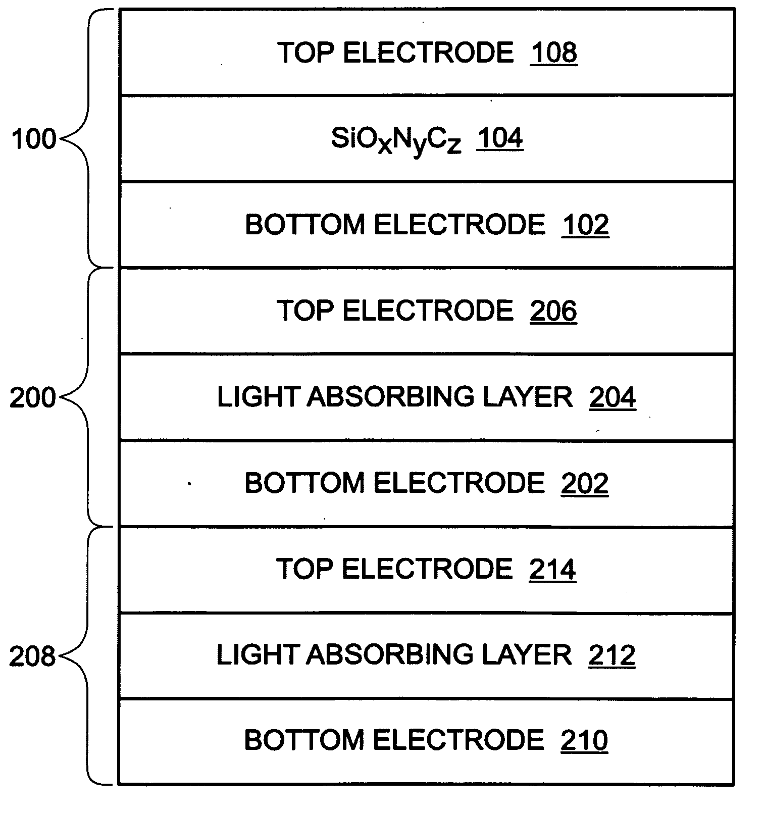
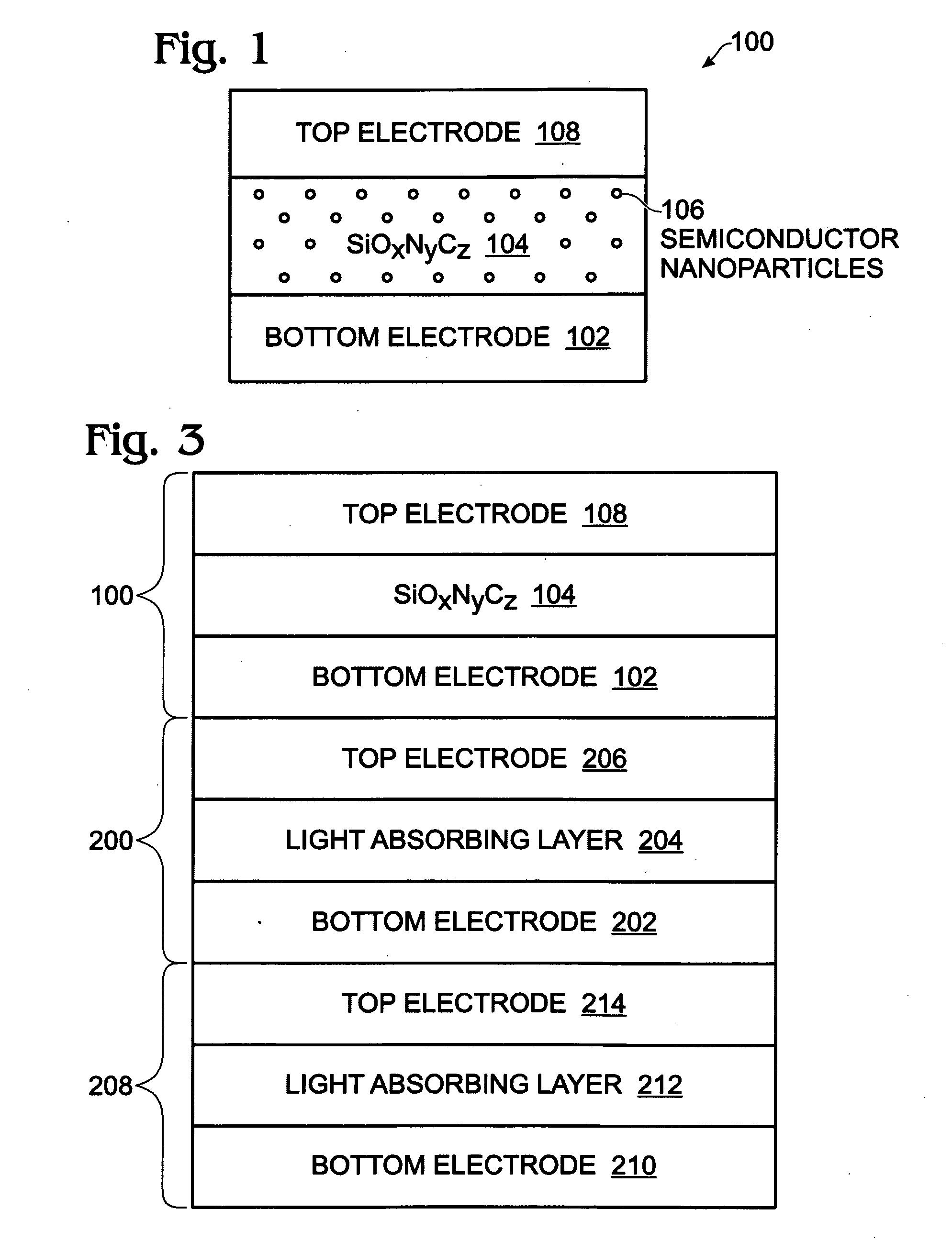
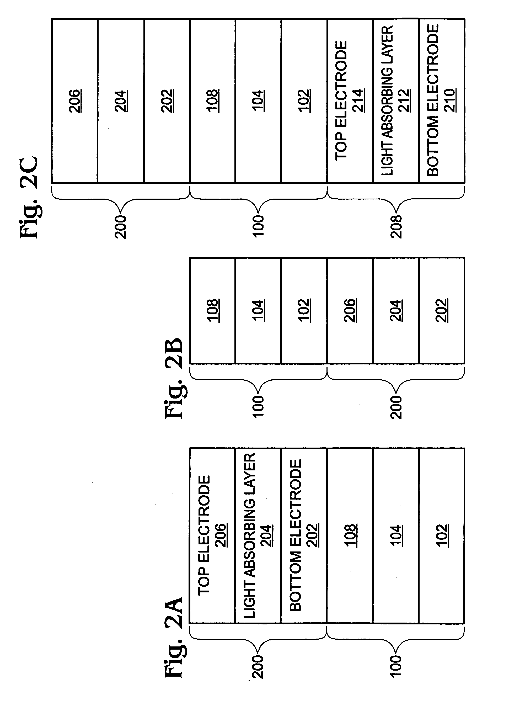
[0036]FIG. 1 is a partial cross-sectional view of a solar cell. The solar cell 100 comprises a bottom electrode 102 doped with either an n-type or p-type dopant. A SiOxNyCz thin film 104 overlies the bottom electrode 102, where x, y, z≧0. The SiOxNyCz thin film 104 has a bandgap in the range of about 1.9 to 3.0, and is embedded with semiconductor nanoparticles 106, which may be Si, Ge, or a combination of Si and Ge. In one aspect, the semiconductor nanoparticles 106 have a size in the range of 1 to 20 nanometers (nm). A doped top electrode 108 overlies the SiOxNyCz thin film 104. If the bottom electrode 102 is n-doped, the top electrode 108 is p-doped. Alternately, if the bottom electrode 102 is p-doped, the top electrode 108 is n-doped.

[0037]In one aspect, the SiOxNyCz thin film 104 is either a doped or an intrinsic material. For example, the SiOxNyCz thin film 104 may be embedded with a dopant such as a Type 3, Type 4, Type 5, or rare earth elements. The use of such a dopant may a...


PUM

PropertyMeasurementUnit
Temperatureaaaaaaaaaa
Pressureaaaaaaaaaa

Abstract

A solar call is provided along with a method for forming a semiconductor nanocrystalline silicon insulating thin-film with a tunable bandgap. The method provides a substrate and introduces a silicon (Si) source gas with at least one of the following source gases: germanium (Ge), oxygen, nitrogen, or carbon into a high density (HD) plasma-enhanced chemical vapor deposition (PECVD) process. A SiOxNyCz thin-film embedded with a nanocrystalline semiconductor material is deposited overlying the substrate, where x, y, z≧0, and the semiconductor material is Si, Ge, or a combination of Si and Ge. As a result, a bandgap is formed in the SiOxNyCz thin-film, in the range of about 1.9 to 3.0 electron volts (eV). Typically, the semiconductor nanoparticles have a size in a range of 1 to 20 nm.

Description

RELATED APPLICATIONS[0001]This application is a continuation-in-part of a pending patent application entitled, SILICON OXIDE THIN-FILMS WITH EMBEDDED NANOCRYSTALLINE SILICON, invented by Pooran Joshi et al., Ser. No. 11 / 418,273, Attorney Docket No. SLA963, filed May 4, 2006, which is a continuation-in-part of the following patent applications:[0002]ENHANCED THIN-FILM OXIDATION PROCESS, invented by Pooran Joshi et al., Ser. No. 11 / 327,612, Attorney Docket No. SLA8012, filed Jan. 6, 2006, pending;[0003]HIGH-DENSITY PLASMA HYDROGENATION, invented by Pooran Joshi et al., Ser. No. 11 / 013,605, Attorney Docket No. SLA0880, filed Dec. 15, 2004, issued as U.S. Pat. No. 7,446,023;[0004]DEPOSITION OXIDE WITH IMPROVED OXYGEN BONDING, invented by Pooran Joshi, Ser. No. 10 / 801,377, Attorney Docket No. SLA0766, filed Mar. 15, 2004, issued as U.S. Pat. No. 7,122,487;[0005]HIGH-DENSITY PLASMA OXIDATION FOR ENHANCED GATE OXIDE PERFORMANCE, invented by Joshi et al., Ser. No. 11 / 139,726, Attorney Docke...

Claims


Application Information

Patent Timeline
IPC IPC(8): H01L31/042H01L21/205H01L31/028
CPCC23C16/30C23C16/5096C23C16/56H01L21/02126H01L21/02274H01L21/02321H01L33/42H01L21/0234H01L21/02532H01L21/02601H01L21/0262H01L21/31608H01L21/02337Y02E10/547
Inventor JOSHI, POORAN CHANDRAVOUTSAS, APOSTOLOS T.
Owner SHARP KK
Why Eureka
Try Eureka