
Coaxial microwave assisted deposition and etch systems

Inactive Publication Date: 2009-09-24
APPLIED MATERIALS INC
View PDF80 Cites 25 Cited by
  • Summary
  • Abstract
  • Description
  • Claims
  • Application Information

AI Technical Summary

Benefits of technology

[0006]Embodiments of the present invention provide systems for achieving improved film properties by introducing additional processing parameters, such as a movable position for the microwave source and pulsing power to the microwave source, and extending the operational ranges and processing windows with the assistance of the microwave source. Embodiments of the invention use a coaxial microwave antenna for radiating microwaves to assist in physical vapor deposition (PVD) or chemical vapor deposition (CVD) systems. One aspect of the present invention is that the system uses a coaxial microwave antenna inside a processing chamber, with the antenna being movable between a substrate and a plasma source, such as a sputtering target, a planar capacitively generated plasma source, or an inductively coupled source. In a special case when only a microwave plasma source is present, the position of the microwave antenna is movable relative to a substrate. The coaxial microwave antenna adjacent to the plasma source can assist the ionization more homogeneously and allow substantially uniform deposition over large areas. Another aspect of the invention is that the antenna may be subjected to a pulsing power for increasing plasma efficiency over a continuous power.
[0011]Embodiments of the invention also include a movable microwave antenna inside a processing chamber. In one specific embodiment of the invention, the antenna is near the target for increasing the plasma density of radical species and reducing energy broadening. In another specific embodiment of the invention, the antenna is approximately in the middle of the processing chamber for enhancing bulk plasma properties. In a third specific embodiment of the invention, the antenna is near the substrate to affect film properties such as density and edge coverage.
[0012]The potential areas of application by the present invention include solar cells (e.g. deposition of amorphous and microcrystalline photovoltaic layers with band gap controllability and increased deposition rates); plasma display devices (e.g. deposition of dielectric layers with energy savings and lower manufacturing cost); scratch resistant coatings (e.g. thin layers of organic and inorganic materials on polycarbonate for UV absorption and scratch resistance); advanced chip-packaging plasma cleaning and pretreatment (e.g. the advantages are zero static charge buildup and without UV radiation damage); semiconductors, alignment layers, barrier films, optical films, diamond like carbon and pure diamond films, where improved barriers and scratch resistance can be achieved by using the present invention.

Problems solved by technology

However, a drawback is that magnetized plasma tends to have larger variations in plasma density, because the strength of the magnetic field significantly varies with distance.
This non-homogeneity may cause complications for deposition of large areas.
The ionization of atoms requires a high density plasma, which makes it difficult for the deposition atoms to escape without being ionized by energetic electrons.
Capacitively generated plasmas are usually very lightly ionized, resulting in low deposition rate.
A drawback with this technique is that ions with about 100 eV in energy bombard the coil, erode the coils and then generate sputtered contaminants that may adversely affect the deposition.
Also, the high energy of the ions may cause damage to the substrate.
However, this technique does not provide a homogeneous assist to enhance plasma generation.
It also does not provide enough plasma density to sustain its own discharge without the assistance of the sputtering cathode.
Additionally, scale up of such systems for large area deposition is limited to a length on the order of 1 meter or less due to non-linearity.

Method used


Image

  • Coaxial microwave assisted deposition and etch systems
  • Coaxial microwave assisted deposition and etch systems
  • Coaxial microwave assisted deposition and etch systems

Examples


Embodiment Construction

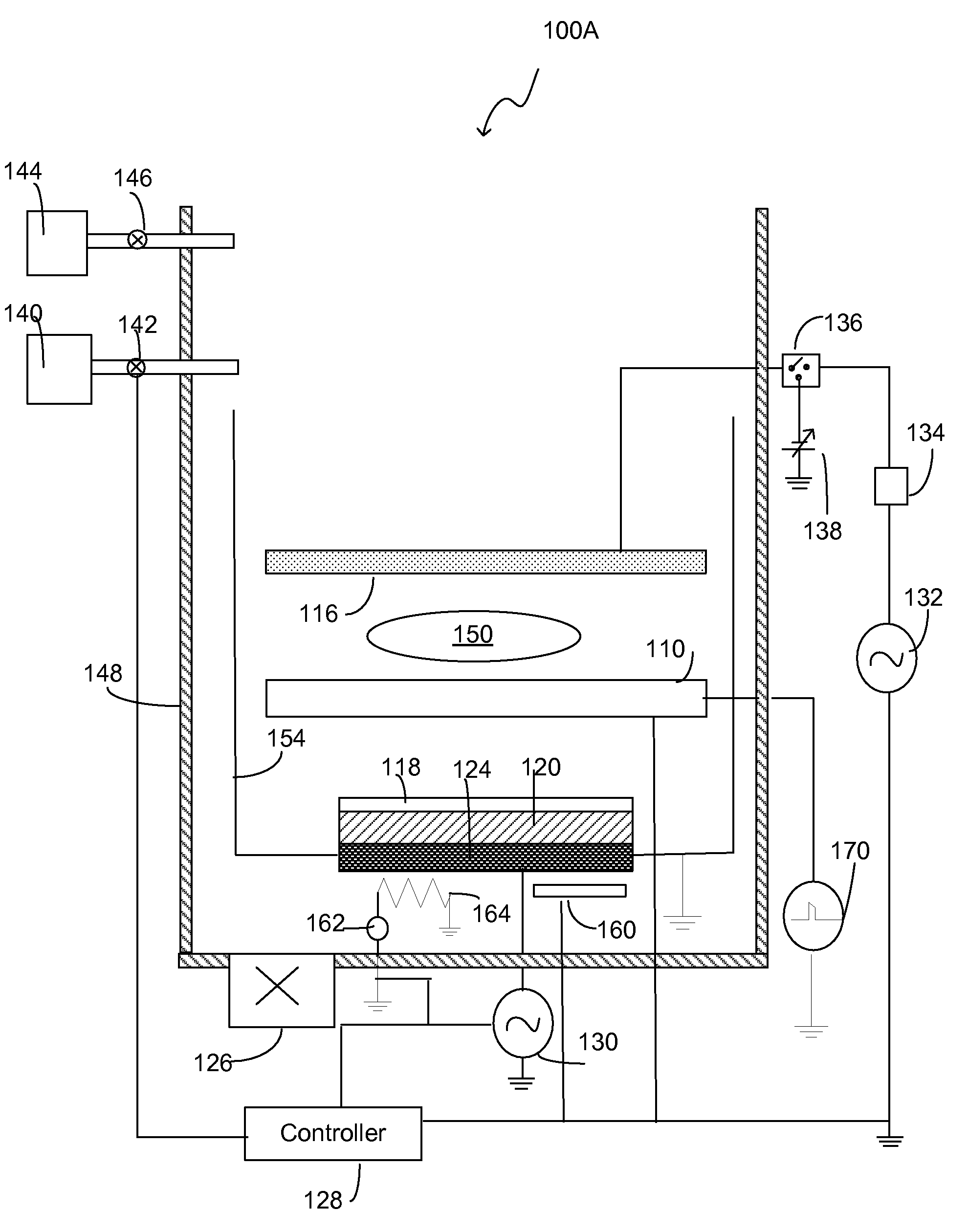
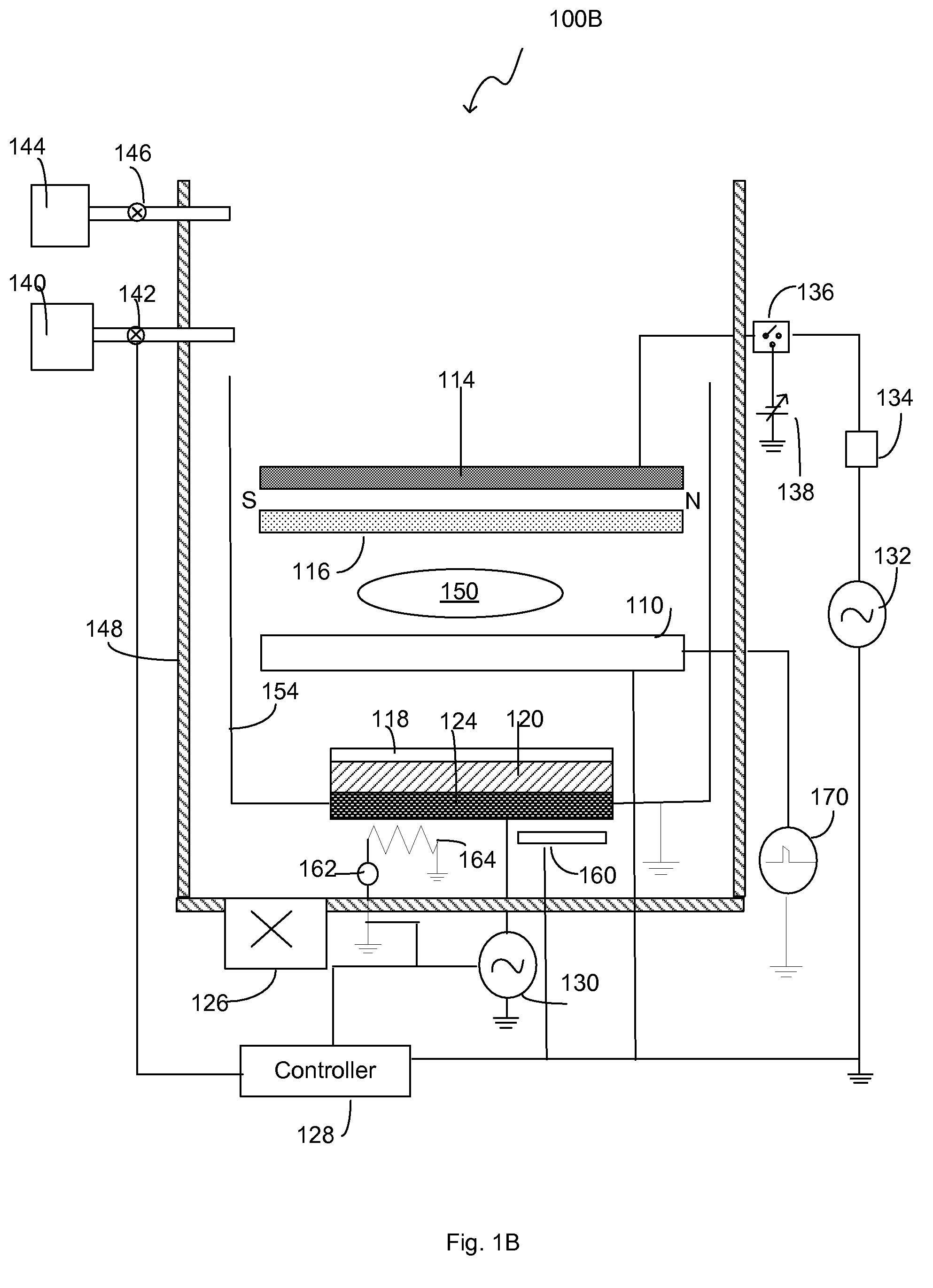
1. Overview of Microwave Assisted Deposition

[0026]Microwave plasma has been developed to achieve higher plasma densities (e.g. 1012 ions / cm3) and higher deposition rates, as a result of improved power coupling and absorption at 2.45 GHz when compared to a typical radio frequency (RF) coupled plasma sources at 13.56 MHz. One drawback of the RF plasma is that a large portion of the input power is dropped across the plasma sheath (dark space). By using microwave plasma, a narrow plasma sheath is formed and more power can be absorbed by the plasma for creation of radical and ion species, which increases the plasma density and reduces collision broadening of the ion energy distribution to achieve a narrow energy distribution.

[0027]Microwave plasma also has other advantages such as lower ion energies with a narrow energy distribution. For instance, microwave plasma may have low ion energy of 1-25 eV, which leads to lower damage when compared to RF plasma. In contrast, standard planar disc...


PUM

PropertyMeasurementUnit
Dielectric polarization enthalpyaaaaaaaaaa
Poweraaaaaaaaaa
Densityaaaaaaaaaa

Abstract

Disclosed are systems for achieving improved film properties by introducing additional processing parameters, such as a movable position for the microwave source and pulsing power to the microwave source, and extending the operational ranges and processing windows with the assistance of the microwave source. A coaxial microwave antenna is used for radiating microwaves to assist in physical vapor deposition (PVD) or chemical vapor deposition (CVD) systems. The system may use a coaxial microwave antenna inside a processing chamber, with the antenna being movable between a substrate and a plasma source, such as a sputtering target, a planar capacitively generated plasma source, or an inductively coupled source. In a special case when only a microwave plasma source is present, the position of the microwave antenna is movable relative to a substrate. The coaxial microwave antenna adjacent to the plasma source can assist the ionization more homogeneously and allow substantially uniform deposition over large areas.

Description

BACKGROUND OF THE INVENTION[0001]Glow discharge thin film deposition processes are extensively used for industrial applications and materials research, especially in creating new advanced materials. Although chemical vapor deposition (CVD) generally exhibits superior performance for deposition of material in trenches or holes, physical vapor deposition (PVD) is sometimes preferred because of its simplicity and lower cost. In PVD, magnetron sputtering is often preferred, as it may have a 100 times increase in deposition rate and a 100 times lower required discharge pressure than non-magnetron sputtering. Inert gases, especially argon, are usually used as sputtering agents because they do not react with target materials. When a negative voltage is applied to a target, positive ions, such as positively charged argon ions, hit the target and knock the atoms out. Secondary electrons are also ejected from the target surface. The magnetic field can trap the secondary electrons close to the...

Claims


Application Information

Patent Timeline
IPC IPC(8): H05H1/30C23C16/511H01L21/3065
CPCC23C14/34C23C14/345C23C14/3485C23C16/511C23C16/515H05H1/46H01J37/321H01J37/32192H01J37/3222H01J37/3408H01J37/32091
Inventor STOWELL, MICHAEL W.KRISHNA, NETYHOFMANN, RALFGRIFFITH, JOE
Owner APPLIED MATERIALS INC
Features
  • Generate Ideas
  • Intellectual Property
  • Life Sciences
  • Materials
  • Tech Scout
  • Unparalleled Data Quality
  • Higher Quality Content
  • 60% Fewer Hallucinations
Learn More