Oxide superconductor and method of fabricating same

a superconductor and oxide technology, applied in the direction of superconducting magnets/coils, superconductor devices, magnetic bodies, etc., can solve the problems of inability to achieve excellent superconductors, inability to find effective residual carbon reduction techniques, and inability to meet the requirements of high crystallinity

Active Publication Date: 2009-10-01
KK TOSHIBA
View PDF7 Cites 25 Cited by
  • Summary
  • Abstract
  • Description
  • Claims
  • Application Information

AI Technical Summary

Benefits of technology

[0023]In accordance with one aspect of this invention, an oxide superconductor is provided, which includes a substrate, and an oxide superconductor film which is formed on the substrate to have high crystallinity, wherein a <001> direction of crystal grains is oriented substantially perpendicularly to the substrate and wherein (100) planes of neighboring ones of the crystal grains are oriented to form therebetween an oblique angle ranging from zero to four degrees or ranging from eighty-six to ninety degrees. The oxide superconductor film has a multilayer structure made up of a plurality of high-density magnetic field trap layers stacked in almost parallel to the substrate and a low-density magnetic field trap layer interposed between adjacent ones of the high-density magnetic field trap layers. An average grain boundary width of the high-density magnetic field trap layers in a cross-section horizontal to the substrate is less than or equal to eighty nanometers. The average grain boundary width is less than an average grain boundary width of the low-density magnetic field trap layer in its cross-section horizontal to the substrate.
[0024]In accordance with another aspect of the invention, an oxide superconductor fabrication method is provided, which includes the steps of preparing as a coating solution a

Problems solved by technology

However, later studies have revealed the fact that the in-situ process suffers from difficulties in obtaining excellent superconductors as it strictly requires that all of the film fabrication conditions must be set up together at a time.
The ex-situ process, on the other hand, was first considered to have the risk of manufacturing cost increase.
However, as this technique uses no carbon, any residual carbons do not exist in the resultant superconductor at all.
However, an effective residual carbon reduction technique is not found yet.
This leads to a decrease in critical current density Jc.
As well known among those skilled in the art, magnetic fluxes that form a magnetic field cause superconduction properties to be impaired at every part if these magnetic fluxes are movable within supercurrent-obtainable regions.
This would result in significant deterioration of superconductor wire characteristics to one-hundredth ( 1/100) or below as a whole.
However, it is also known that when introducing a certain material with no supercurrent flowability, such as BaZrO3, into YBa2Cu3O7-x superconductor to thereby form a film, followed by execution of pure oxygen anneal for converting the superconductor from a tetragonal crystal structure into an orthorhombic crystal structure, the resulting superconduction properties are badly affected

Method used


Image

  • Oxide superconductor and method of fabricating same
  • Oxide superconductor and method of fabricating same
  • Oxide superconductor and method of fabricating same

Examples


first embodiment

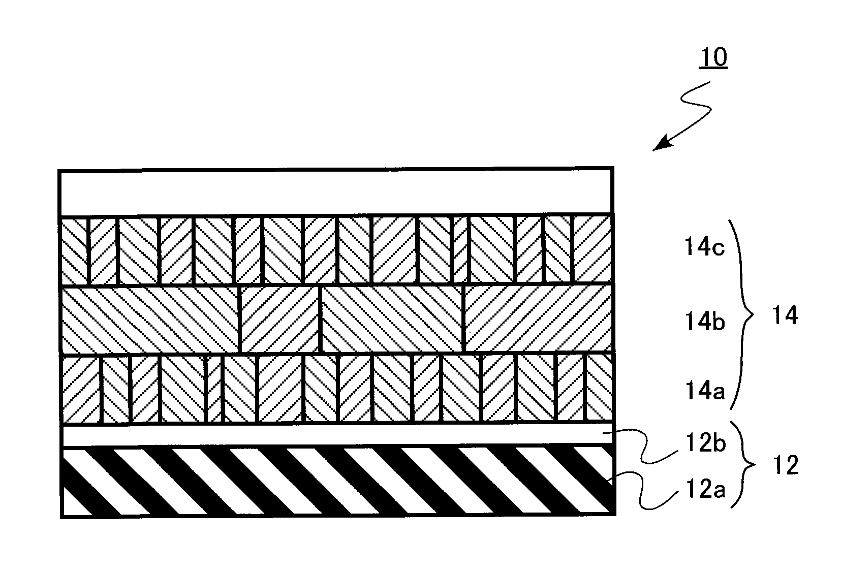
[0042]An oxide superconductor structure in accordance with first embodiment of this invention includes a substrate, and an oxide superconductor film which is formed on the substrate to have high crystallinity with a direction of crystal grains being oriented substantially perpendicularly to the substrate and with (100) planes of neighboring ones of the crystal grains being oriented to form therebetween an oblique angle ranging from zero to four degrees or ranging from eighty-six to ninety degrees. The oxide superconductor film has a multilayer structure made up of a plurality of high-density magnetic field trap layers stacked in almost parallel to the substrate and a low-density magnetic field trap layer which is interposed between adjacent ones of the high-density magnetic field trap layers. An average grain boundary width of the high-density magnetic field trap layers in a cross-section horizontal to the substrate is less than or equal to eighty nanometers. This average grain bou...

second embodiment

[0095]A fabrication method of an oxide superconductor structure in accordance with second embodiment of this invention is includes the steps of preparing as a coating solution a fluorocarboxylate-methanol solution with a mixture of barium and copper plus at least one metal which is selected from the group consisting of yttrium and lanthanoids with cerium, praseodymium, promethium and lutetium being excluded therefrom, laying the coating solution on a substrate to form a gel film, applying calcining process to the gel film to thereby form a calcined film, and applying to the calcined film firing process with more than two changes in gas flow rate during thermal processing and oxygen anneal to thereby convert the calcined film into an oxide film. This embodiment method is similar to the first embodiment with the humidification amount being replaced by the gas flow rate for being changed during the firing process.

[0096]As previously stated in conjunction with the first embodiment, it i...

examples

[0098]Practically implemented examples of this invention will be described below.

Preliminary Experiment 1

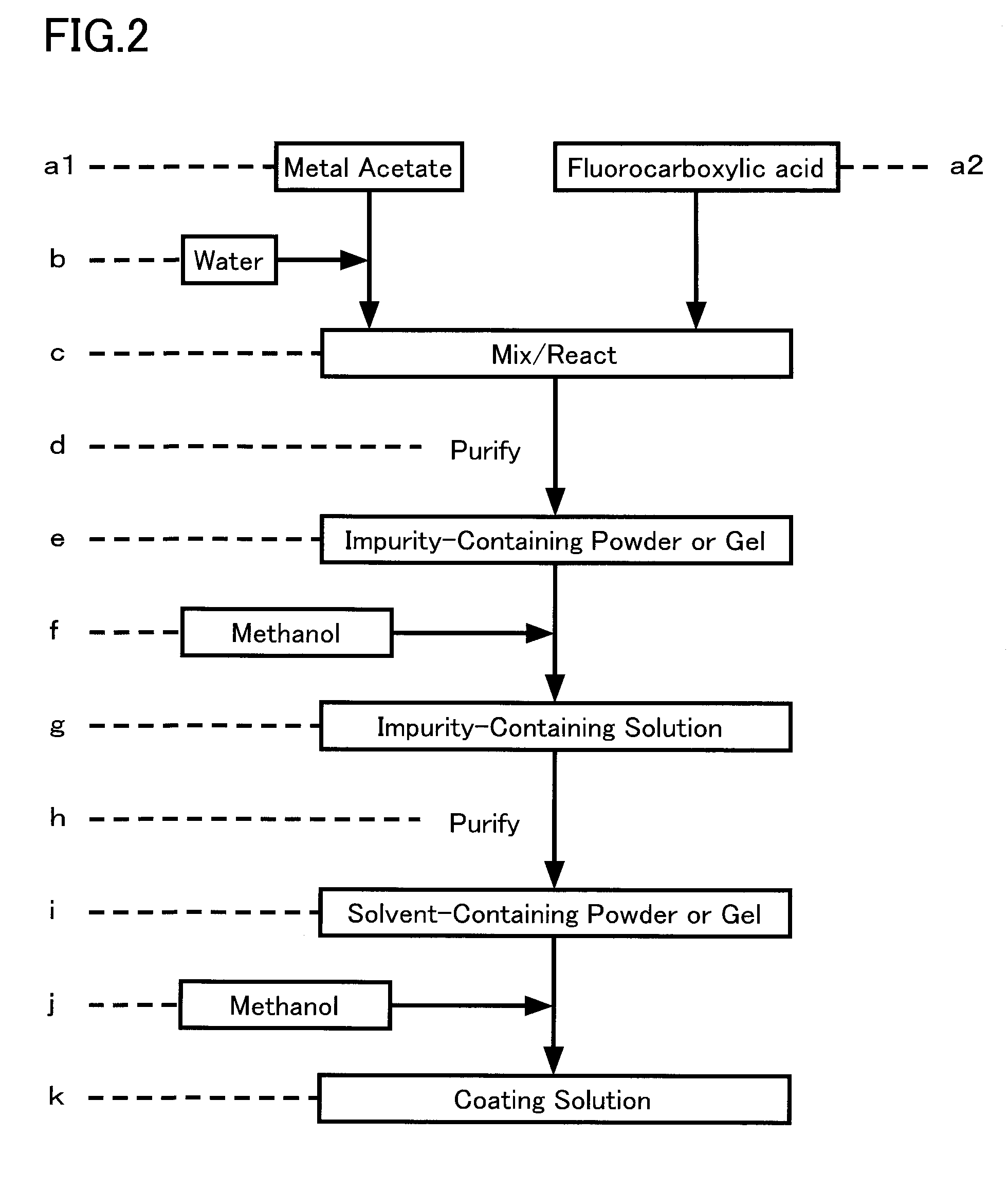
[0099]Firstly, experimentation was carried out to clarify the relationship of low-angle grain boundary width in oxide superconductor film versus superconductivity properties. Powders of hydrates of Y(OCOCH3)3, Ba(OCOCH3)2 and Cu(OCOCH3)2 were dissolved into ion-exchange water, respectively. Each was then mixed with a reaction-equivalent molar quantity of CF3COOH, followed by stirring thereof. Then, these were blended together at a metal ion molar ratio of 1:2:3, thereby obtaining a mixed solution. This mixed solution was put into an eggplant-shaped flask for performing reaction and purification for twelve (12) hours at a reduced pressure in a rotary evaporator, thus obtaining a semitransparent blue-colored gel or sol.

[0100]The resultant gel or sol was added with methanol (at step “f” of FIG. 2) having its weight equivalent to a hundredfold increase of that of the gel or sol, for ...


PUM

PropertyMeasurementUnit
Angleaaaaaaaaaa
Angleaaaaaaaaaa
Angleaaaaaaaaaa

Abstract

An oxide superconductor with superconduction properties being improved by effectively introducing a pinning center thereinto and its fabrication method are disclosed. The superconductor has a high-crystallinity oxide superconductor film which is formed on a substrate with a <001> direction of crystal grain being oriented almost perpendicularly to the substrate and with (100) planes of neighboring crystal grains being oriented to form an oblique angle ranging from 0 to 4 degrees or 86 to 90 degrees. The film has a multilayer structure including a plurality of high-density magnetic field trap layers stacked in almost parallel to the substrate and a low-density magnetic field trap layer sandwiched therebetween. An average grain boundary width of the high-density trap layers in a cross-section horizontal to the substrate is 80 nm or less. The width is less than an average grain boundary width of the low-density trap layer in its cross-section horizontal to the substrate.

Description

CROSS-REFERENCE TO RELATED APPLICATION[0001]This application is based upon and claims priority to Japanese Patent Application No. 2008-082683, filed Mar. 27, 2008, the entire contents of which are incorporated herein by reference.FIELD OF THE INVENTION[0002]The present invention relates generally to an oxide superconductor adaptable for use in various applications including, but not limited to, lengthy electrical wires, superconducting coils, superconduction magnets, magnetic resonance imaging (MRI) systems, magnetic levitation or “maglev” trains, and superconductor magnetic energy storage (SMES) devices. This invention also relates to a method of making the oxide superconductor.BACKGROUND OF THE INVENTION[0003]In recent years, high critical current oxide superconducting materials are under diligent investigation for practical implementation. Such oxide superconductors hold great promise for application to long electrical wires, nuclear fusion reactors, maglev trains, accelerators, ...

Claims


Application Information

Patent Timeline
IPC IPC(8): H01L39/12H01L39/24
CPCH01L39/143H01L39/2451H01L39/2425H10N60/203H10N60/0324H10N60/0548
Inventor HAYASHI, MARIKOARAKI, TAKESHI
Owner KK TOSHIBA
Why Eureka
Try Eureka