Wide band gap semiconductor device and method for producing the same

a semiconductor device and wide band gap technology, applied in semiconductor devices, diodes, electrical equipment, etc., can solve the problems of complex circuit configuration, unsuitable for high-speed switching, cost increase, etc., and achieve the effect of improving avalanche breakdown tolerance at turning-off time, short reverse recovery time, and low resistan

Active Publication Date: 2009-11-19
FUJI ELECTRIC CO LTD
View PDF7 Cites 88 Cited by
  • Summary
  • Abstract
  • Description
  • Claims
  • Application Information

AI Technical Summary

Benefits of technology

[0040]According to the invention, trenches are formed both in a Schottky barrier diode part and in a gate electrode part so that the trenches are close to each other, and the trench (second trench) in the Schottky barrier diode part is formed so as to be deeper than the trench (first trench) in the gate electrode part. Moreover, a metal electrode is formed in the second trench in the Schottky barrier diode part so that the metal electrode comes into Schottky contact with the surface of the n base layer exposed in the bottom of the second trench. In this manner, in a trench MOSFET using a wide band gap semiconductor, a low on-resistance can be provided and a built-in Schottky barrier diode having a short reverse recovery time can be formed easily. Moreover, a p-type region is formed in part of the second trench of the built-in Schottky barrier diode part being in contact with the surface of the n base layer, preferably in the bottom of the second trench so that avalanche breakdown tolerance at turning-off time c...

Problems solved by technology

Bipolar transistors or IGBTs (insulated gate bipolar transistors) are capable of gaining high current density, but unsuited to high-speed switching.
Consequently, the circuit configuration is complicated and the apparatus size is enlarged, so that the cost increases.
However, the complementary IGBT module has not been put into practice currently.
The reason is that the complementary IGBT module is so low in avalanche breakdown tolerance that there arises a problem that the bipolar operation of the p-channel IGBTs leads to device breakdown theoretically soon (IEEE Transaction on Electron Devices, Vol. 38, p.
However, such a complementary MOSFET module has not been available on the market yet because MOSFETs have a disadvantage of being apt to be very high in on-resistance compared with the IGBTs so that the loss produced in the MOSFETs is large.
In this case, there is, however, a problem that switching loss still increases because the reverse recovery time of the built-in PIN diode is delayed by implantation of minority carriers even when the built-in PIN diode is electrically connected as the FWD.
It is, however, very difficult to produce a low-resistance low-defect-density p-type semiconductor substrate from a wide band gap semiconductor, especially from SiC or GaN.
For this reason, there arises a problem that on-resistance cannot be reduced sufficiently because the potential drop in the p-type semiconductor substrate is large even when the p-type semiconductor substrate is used for forming a p-channel MOSFET.
On the other hand, the SiC trench MOSFET has a problem that a very diff...

Method used


Image

  • Wide band gap semiconductor device and method for producing the same
  • Wide band gap semiconductor device and method for producing the same
  • Wide band gap semiconductor device and method for producing the same

Examples


embodiment 1

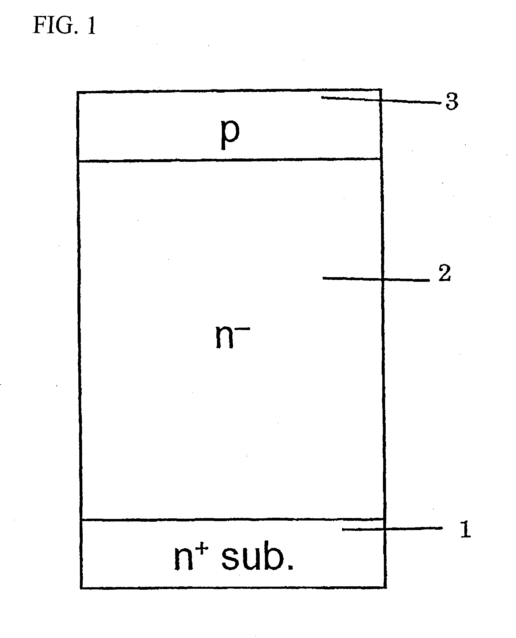
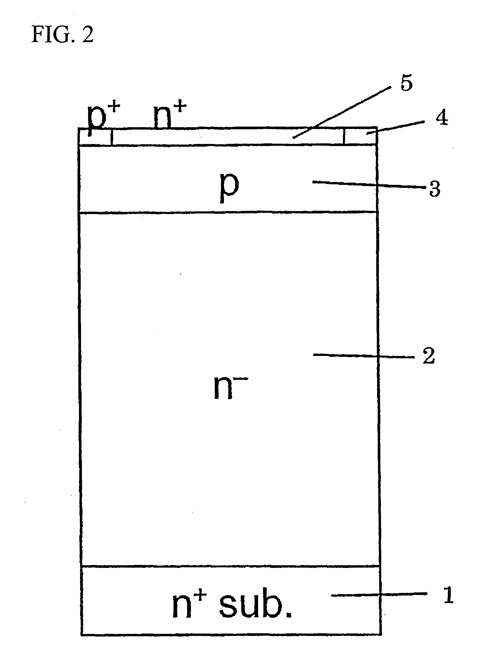
[0086]Embodiment 1 of the invention will be described below with reference to FIGS. 1 to 5. In Embodiment 1, a trench MOSFET which exhibits a withstand voltage of 1200 V and which has an active region located in the center so that a main current flows in the active region, and a peripheral voltage withstanding structure region disposed to surround the active region is provided as a vertical trench gate MOS power semiconductor device. First, n-type SiC substrate 1 (referred to as “n+ sub.” in FIGS. 1 to 5) with a sufficiently high impurity concentration is prepared. In this embodiment, the SiC substrate contains about 2×1018 cm−3 of nitrogen as an impurity. N-type SiC drift layer 2 containing about 1.0×1016 cm−3 of nitrogen and p-type SiC base layer 3 containing about 2.1×1017 cm−3 of aluminum are epitaxially grown on SiC substrate 1 so that the thicknesses of layers 2 and 3 are about 10 μm and 2.5 μm respectively (FIG. 1). Incidentally, FIG. 1 shows neither the actual thicknesses of...

embodiment 2

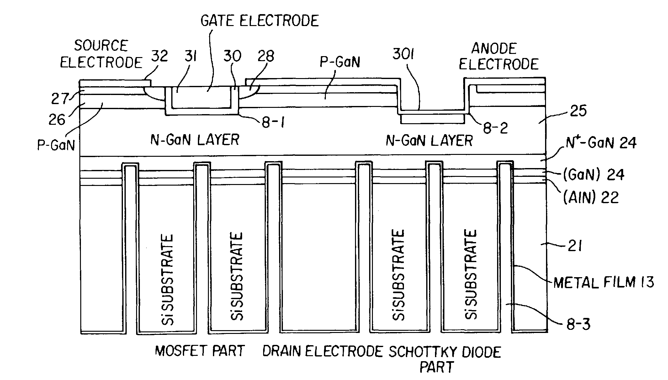
[0130]A wide band gap semiconductor device according to Embodiment 2 of the invention, especially, a trench MOS device will be described below with reference to FIGS. 15 to 19. In Embodiment 2, a GaN trench MOSFET with a withstand voltage of 600 V is used as a vertical trench gate type MOS power semiconductor device. The point of difference from the GaN trench MOSFET according to Embodiment 1 is that an Si substrate is used as a semiconductor substrate with a high impurity concentration. First, as shown in FIG. 15, Si substrate 21 having (111) face as a principal surface is prepared as the Si substrate so that AlN layer 22 and non-doped GaN layer 23 as buffer layers on which GaN layers 24, 25 and 26 will be further grown are formed on Si substrate 21 by a metal organic chemical vapor deposition method (MOCVD) which is a commonly known technique. Because the grating constant of the Si (111) face is 0.3840 nm and the grating constant of GaN is 0.3819 nm which is a value relatively nea...

embodiment 3

[0140]Embodiment 3 of the invention will be described below with reference to FIGS. 20 to 24. Incidentally, in Embodiment 3, an SiC p-channel type trench MOSFET with a withstand voltage of 1200 V is provided as a vertical trench gate MOS power semiconductor device. First, n-type SiC substrate 41 is prepared. In this embodiment, SiC substrate 41 is provided as a high-resistance n-type SiC substrate containing about 2×1014 cm−3 of nitrogen as an impurity. P-type SiC layer 42 containing about 1.0×1019 cm−3 of nitrogen and p-type SiC drift layer 43 containing about 1.0×1016 cm−3 of nitrogen are epitaxially grown on SiC substrate 41 so that the thicknesses of layers 42 and 43 are about 2 μm and 10 μm respectively. N-type SiC base layer 44 containing about 2.1×1017 cm−3 of nitrogen is epitaxially grown on p-type SiC drift layer 43 so that the thickness of layer 44 is 2.5 μm (FIG. 20). N+ contact region 45 (FIG. 21) and p+ source region 46 (FIG. 22) are formed by selective ion implantation...


PUM


Abstract

A wide band gap semiconductor device is disclosed. A first trench in a gate electrode part and a second trench in a source electrode part (Schottky diode part) are disposed so that the first and second trenches are close to each other while and the second trench is deeper than the first trench. A metal electrode is formed in the second trench to form a Schottky junction on a surface of an n-type drift layer in the bottom of the second trench. Further, a p+-type region is provided in part of the built-in Schottky diode part being in contact with the surface of the n-type drift layer, preferably in the bottom of the second trench. The result is a wide band gap semiconductor device which is small in size and low in on-resistance and loss, and in which electric field concentration applied on a gate insulating film is relaxed to suppress lowering of withstand voltage to thereby increase avalanche breakdown tolerance at turning-off time.

Description

BACKGROUND OF THE INVENTION[0001]A. Field of the Invention[0002]The present invention relates to a high withstand voltage semiconductor device using a wide band gap semiconductor such as silicon carbide semiconductor (hereinafter abbreviated to as SiC) or gallium nitride semiconductor (hereinafter abbreviated to as GaN) with a wider band gap than the band gap of silicon semiconductor (hereinafter abbreviated to Si), and a method for producing the same.[0003]B. Description of the Related Art[0004]In many cases, Si has been heretofore used as a semiconductor substrate material of a power semiconductor device for controlling a large current while withstanding a high voltage. There are several kinds of Si power semiconductor devices. At present, the several kinds of Si power semiconductor devices are used for various purposes. Bipolar transistors or IGBTs (insulated gate bipolar transistors) are capable of gaining high current density, but unsuited to high-speed switching. For example, ...

Claims


Application Information

Patent Timeline
IPC IPC(8): H01L29/20H01L29/24H01L21/28
CPCH01L29/0623H01L29/7839H01L29/0657H01L29/0661H01L29/0696H01L29/1608H01L29/2003H01L29/41766H01L29/45H01L29/452H01L29/47H01L29/475H01L29/66068H01L29/66734H01L29/7806H01L29/7811H01L29/7813H01L29/401H01L29/7827H01L29/0653
Inventor IWAMURO, NORIYUKI
Owner FUJI ELECTRIC CO LTD
Why Eureka
Try Eureka